5 external memory interfaces, 1 sdram controller, Chapter 5. external memory interfaces -1 – Cirrus Logic CS4970x4 User Manual
Page 86: 1 sdram controller -1, Figure 5-1. sdram interface block diagram -1, Chapter 5, "external, Memory interfaces

SDRAM Controller
CS4953x4/CS4970x4 System Designer’s Guide
DS810UM6
Copyright 2013 Cirrus Logic, Inc
5-1
Chapter 5
External Memory Interfaces
5.1 SDRAM Controller
Products in the CS4953x4/CS4970x4 family that use a 144-pin package support a glueless external
SDRAM interface to extend the data and/or program memory of the DSP during runtime. The CS4953x4/
CS4970x4 SDRAM controller provides two-port access to X, Y, and P memory space, a four-word read
buffer, and a double-buffered four-word write buffer. One SDRAM controller port is dedicated to P memory
space and the second port is shared by X & Y memories. An arbiter is wrapped around the first port to
provide external SDRAM access through both X & Y memory space from 8000h-FFFFh. The second port
is connected to provide external SDRAM access through P memory space from 8000h-FFFFh.
The X/Y port has dual write buffers and a single read buffer. The P memory port has a single read buffer.
One of these buffers contains four 32-bit words (128 bits). Every miss to the read buffer will cause the
SDRAM controller to burst eight 16-bit reads on the SDRAM interface.
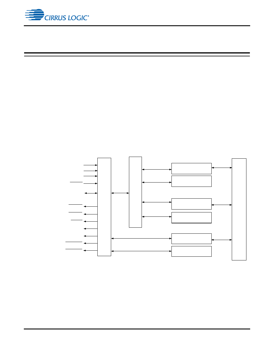
shows a block diagram
of the SDRAM external memory control interface for the CS4953x4/CS4970x4 chip.
Figure 5-1. SDRAM Interface Block Diagram
BA[1:0]
SD_DATA[15:0]
SD_CLKIN
SD_CLKOUT
SD_CAS
SD_DQM0
SD_DQM1
SD_RAS
SD_CLKEN
SD_CS
SD_WE
SDRAM INTERFACE
X RAM
X ROM
Y RAM
Y ROM
P RAM
P ROM
M
E
MOR
Y
CO
NT
ROLLER
X
Y
P
ARBITER
SD_ADDR[12:0]
