4 spi read protocol, 4 spi read protocol -6, Figure 2-4. spi read flow diagram -6 – Cirrus Logic CS4970x4 User Manual
Page 52

SPI Port
CS4953x4/CS4970x4 System Designer’s Guide
DS810UM6
Copyright 2013 Cirrus Logic, Inc
2-6
bytes of any message length, so long as the correct hardware protocol is followed. The example shown in
this section can be generalized to fit any SPI read situation.
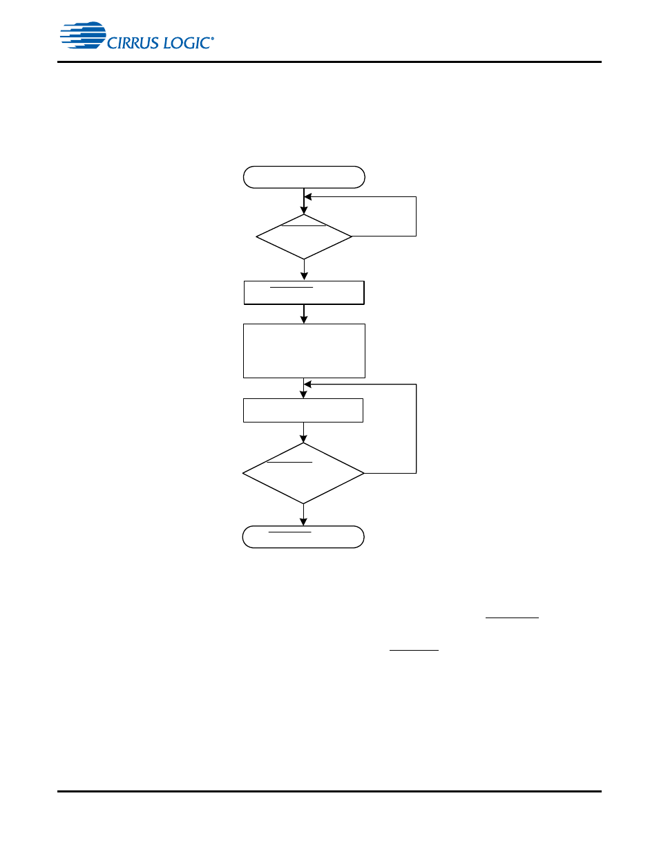
The flow diagram shown in
, illustrates the sequence of events that define the SPI read
protocol. The Serial SPI read protocol is described in
.
Figure 2-4. SPI Read Flow Diagram
2.4.3.4 SPI Read Protocol
1.
A SPI read transaction is initiated by the CS4953x4/CS4970x4 Slave driving SCP1_IRQ low to
indicate that it has data to be read.
2. The Master begins a SPI transaction driving chip select (SCP1_CS) low.
3. This is followed by a 7-bit address and the read/write bit set high for a read. So, the Master should
send 0x81. The 0x81 byte represents the 7-bit SPI address 1000000b, and the least significant bit set
to ‘1’, designates a read.
4. After the falling edge of the serial control clock (SCP1_CLK) for the read/write bit, the Master can
begin clocking out the 4-byte word from the CS4953x4/CS4970x4 on the MISO pin. Data clocked out
of the CS4953x4/CS4970x4 by the Master is valid on the rising edge of SCP1_CLK and data
transitions occur on the falling edge of SCP1_CLK. The serial clock should be held low so that eight
transitions from low-to-high-to-low will occur for each byte.
SCP1_IRQ
(LOW)?
SCP1_IRQ STILL
LOW?
SCP1_CS HIGH
Y
N
Y
N
START
SCP1_CS LOW
READ 4 DATA BYTES
WRITE ADDRESS BYTE
0x81
