P.5.4 control, P.5.4.1 operational mode – Cirrus Logic CS4970x4 User Manual
Page 21

P-10
Copyright 2013 Cirrus Logic, Inc.
DS810UM6
CS40700x Pin Descriptions
CS4953x4/CS4970x4 System Designer’s Guide
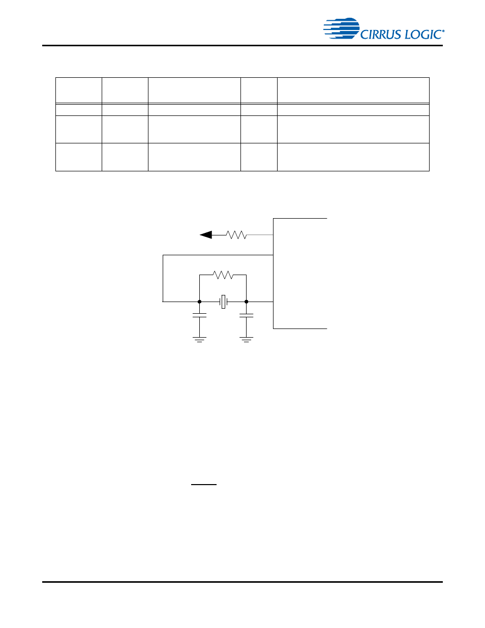
Figure P-4. Crystal Oscillator Circuit Diagram
P.5.4 Control
The CS4953x4/CS4970x4 supports 5 control interface protocols: SPI, I
2
C, Motorola parallel, Intel parallel,
and Multiplexed Intel parallel mode. For modes other than SPI, contact your Cirrus Logic FAE or
representative. All slave serial control modes between the DSP and the host microcontroller use the
Serial Control Port 1 (SCP1) pins. Parallel slave control modes are implemented on the Parallel Control
Port (PCP) pins. A second serial control port (SCP2) is available for master mode applications.
P.5.4.1 Operational Mode
The control interface protocol used is determined by the state of the Hardware Strap pins, HS[4:0] which
are sampled at the rising edge of RESET. The HS[4:0] pins should be pulled to VDD or GND using 10 k
resistors according to the specific control mode desired as shown in
Table 1-1, "Operation Modes" on
.
The following sections describe the pins used for the 5 control modes. For an example diagram of a
system connection, please see
. For information on timing diagrams and
messaging protocol to the CS4953x4/CS4970x4, see
Chapter 1, "Operational Modes"
Table P-7. DSP Core Clock Pins
LQFP-144
Pin #
LQFP-128
Pin #
Pin Name
Pin
Type
Pin Description
123
16
XTAL_OUT
Output
Buffered version of XTI.
124
17
XTI
Input
Reference Clock Input/Crystal Oscillator Input. An
external clock may be input directly to this pin or one
end of a crystal may be connected to this pin.
125
18
XTO
Output
Crystal Oscillator Output. One end of a crystal
oscillator is connected to this pin. This pin cannot be
used to drive external circuitry.
1 Meg
C1
C1
X1
XTI
XTO
XTAL_OUT
To System
CS4953xx
