P.5.2.2 pll, P.5.3 clocking, Cs497xx – Cirrus Logic CS4970x4 User Manual
Page 20

CS40700x Pin Descriptions
CS4953x4/CS4970x4 System Designer’s Guide
DS810UM6
Copyright 2013 Cirrus Logic, Inc
P-9
P.5.2.2 PLL
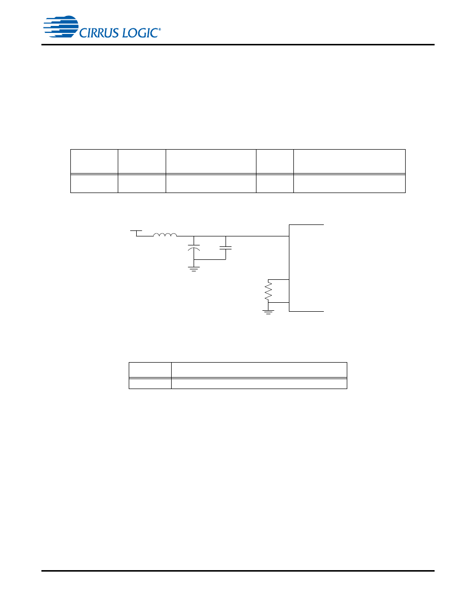
The internal phase locked loop (PLL) of the CS4953x4/CS4970x4 requires an external current reference
resistor. The resistor is used to calibrate the PLL and must meet the tolerances specified below. The
layout topology is shown in the typical connection diagrams. Care should be taken when laying out the
current sense circuitry to minimize trace lengths between the DSP and resistor, and to keep high-
frequency signals away from the resistor. Any noise coupled onto the these traces will be directly coupled
into the PLL, which could affect performance. Please see tables below for pin numbers and external
component values.
Figure P-3. PLL Filter Topology
P.5.3 Clocking
The CS4953x4/CS4970x4 incorporates a programmable phase locked loop (PLL) clock synthesizer. The
PLL takes an input reference clock and produces all the clocks required to run the DSP and peripherals.
In A/V Receiver designs that require low-jitter clocks, the XTI pin is typically connected to an external
12.288 MHz or 24.576 MHz (recommended) oscillator that is used throughout the system.
The CS4953x4/CS4970x4 has a built-in crystal oscillator circuit. A parallel resonant-type crystal is
connected between the XTI and XTO pins as shown in
. The value of C1 is specific to each
crystal. The CS4953x4/CS4970x4 data sheet specifies acceptable crystal parameters (including C
L
and
ESR). When a crystal is used, XTAL_OUT is used to clock other devices in the system such as the S/
PDIF receiver.
The PLL is controlled by the clock manager in the DSP O/S application software. AN288, “CS4953xx/
CS4953x4/CS4970x4 Firmware User’s Manual” should be referenced regarding what CLKIN input
frequency and PLL multiplier values are supported.
Table P-5. PLL Filter Pins
LQFP-144
Pin #
LQFP-128
Pin #
Pin Name
Pin Type
Pin Description
128
20
PLL_REF_RES
Input
Current Reference Resistor for PLL
filter
Table P-6. Reference PLL Component Values
Symbol
Reference Value
R1
5.1 k
1%
PLL_REF_RES
GNDA
CS497xx
R1
VDDA
3.3V
Bead
10u
0.1u
