1 spi system bus description, 2 spi bus dynamics, Figure 2-2. block diagram of spi system bus -3 – Cirrus Logic CS4970x4 User Manual
Page 49
2-3
Copyright 2013 Cirrus Logic, Inc.
DS810UM6
SPI Port
CS4953x4/CS4970x4 System Designer’s Guide
2.4.1 SPI System Bus Description
The SPI bus is a multi-Master bus. This means that more than one device capable of controlling the bus
can be connected to it. Generation of clock signals on the SPI bus is always the responsibility of Master
devices; each Master generates its own clock signals when transferring data on the bus. Bus clock signals
from a Master cannot be altered by any other device on the bus, otherwise a collision will occur. The Slave
chip-select signals can only be controlled by Master devices.
The CS4953x4/CS4970x4 has two serial ports. The O/S currently supports only Slave mode host
communication on SCP1, and Master mode communication on SCP2 for booting from a SPI Flash.
SCP1_MOSI (Master Out/Slave In) and SCP1_MISO (Master In/Slave Out) are bidirectional lines that
change their behavior depending on whether the device is operating in Master or Slave mode. Only the
Master can drive the MOSI signal while only the Slave can drive the MISO signal.
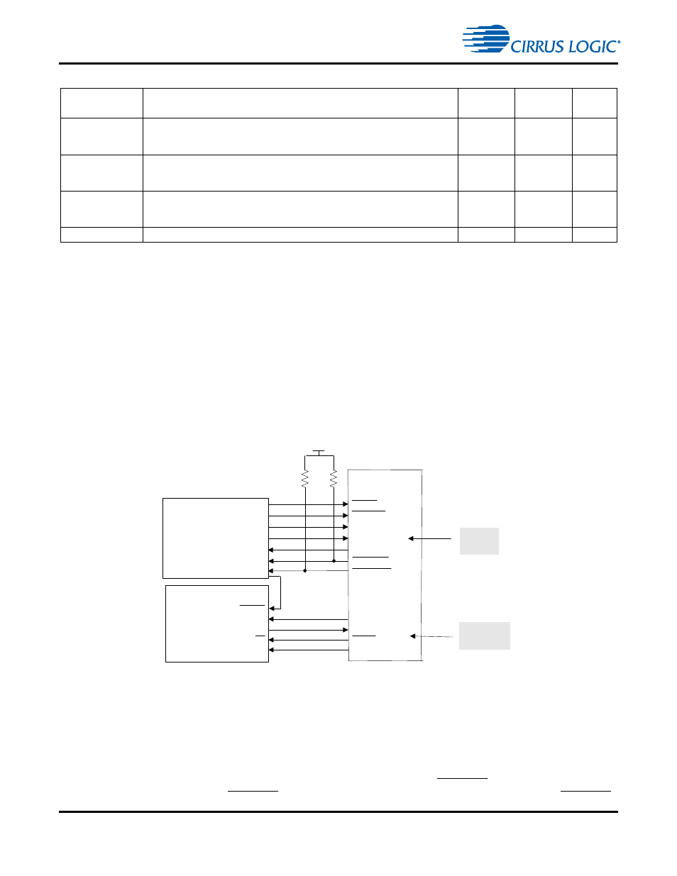
Figure 2-2. Block Diagram of SPI System Bus
As seen in
, two serial ports are available on the CS4953x4/CS4970x4. Each can be configured
to either a Master or Slave. For audio applications, SCP1 is configured as a Slave port and SCP2 is
configured as a Master port. SCP2 is used only in systems that are booting from SPI Flash.
2.4.2 SPI Bus Dynamics
A SPI transaction begins by the Master driving the Slave chip select SCP1_CS low. SPI transactions end
by the Master driving the SCP1_CS high. This SPI bus is considered busy while any device’s SCP1_CS
SCP2_CLK
SPI Control Port Bit Clock
In Master mode, this pin serves as the serial control clock output. In serial Slave
mode, this pin serves as the serial control clock input.
103
1
I/O
SCP2_MISO
SPI Mode Master Data Input/Slave Data Output
In SPI Slave mode this pin serves as the data input. In SPI Master mode this pin
serves as the data output.
105
2
I/O
SCP2_MOSI
SPI Mode Master Data Output/Slave Data Input
SCP2_MOSI in SPI Slave mode this pin serves an the data input, in SPI Master
mode this pin serves as the data output.
106
3
I/O
EE_CS
Master Mode SPI Flash Chip Select, Active Low
25
14
Output
Table 2-1. Serial Control Port SPI Signals (Continued)
Pin Name
Pin Description
LQFP-144
Pin #
LQFP-128
Pin #
Pin Type
RESET
SCP1_CS
SCP1_CLK
SCP1_MOSI
SCP1_MISO
SCP1_IRQ
SCP1_BSY
System
Microcontroller
CS49700x
MOSI
MISO
SPI Flash
MOSI
MISO
RESET
CS
CLK
SCP2_CLK
SCP2_MOSI
SCP2_MISO
EE_CS
3.3k
3.3k
3.3V
MASTER
ONLY
SLAVE
ONLY