AMD SB600 User Manual
Page 267
©2008 Advanced Micro Devices, Inc.
Host PCI Bridge Registers (Device 20, Function 4)
AMD SB600 Register Reference Manual
Proprietary
Page 267
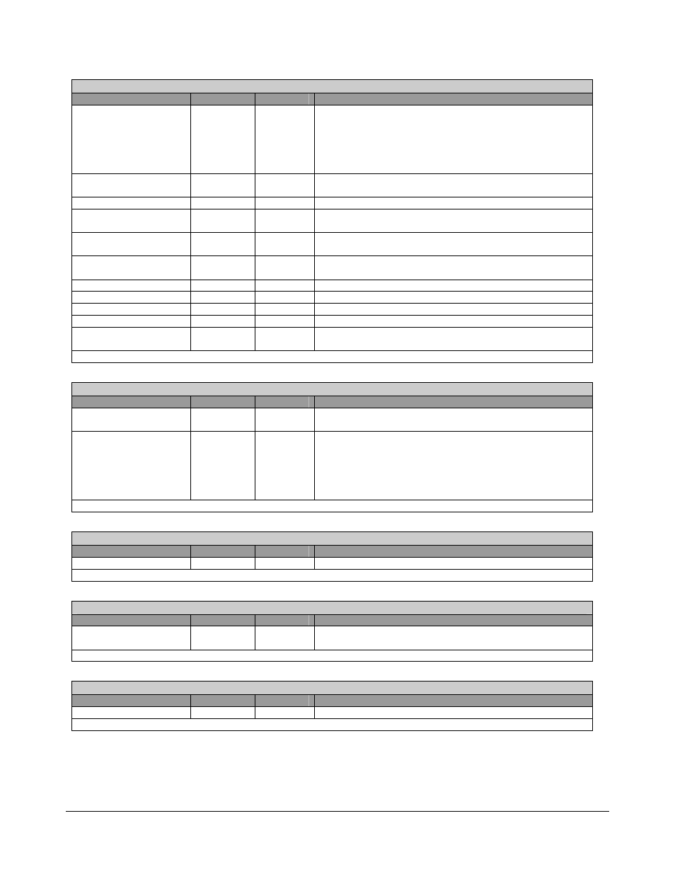
Status- RW - 16 bits - [PCI_Reg: 06h]
Field Name
Bits
Default
Description
Capabilities List
4
0b
Read only. This bit is 1 when Offset 40h [3] = 1. At other
time this bit is 0.
0 – Bridge does not support the Capabilities List
1 – Bridge supports the Capabilities List (Offset 34h is the
pointer to the data structure).
66MHz Capable
5
1b
Hardwired to 1 to indicate PCIB support of 66MHz primary
interface.
Reserved 6
0b
Reserved
Fast Back-to-Back
Capable
7
1b
Hardwired to 1 to indicate PCIB is capable of accepting fast
back-to-back transactions on the primary bus.
Master Parity Error
8
0b
Master Data Parity Error, assertion of P_PERR# (when
PCIB acts as a master) is received, write clears it.
DevSel Timing
9:10
01b
Hardwired to 01b to indicate PCIB will assert DEVSEL# with
medium timing.
Target Abort
11
0b
Signaled Target Abort, write clears it.
Received Target Abort
12
0b
Received Target Abort, write clears it.
Received Master Abort
13
0b
Received Master Abort, write clears it.
Master Abort
14
0b
Signaled System Error bit, write clears it.
Parity Error
15
0b
Detected Parity Error, PCIB detected a parity error and will
assert P_PERR#, write clears it.
PCI device status register.
Revision ID/Class Code- R - 32 bits - [PCI_Reg: 08h]
Field Name
Bits
Default
Description
Revision ID
7:0
00h
These bits are hardwired to 00h to indicate the revision level
of the chip design (for the SB600).
Class Code
31:8
060401h/
060400h
A class code of 06h indicates a bridge device, a subclass
code of 04h indicates PCI bridge and a programming
interface of ‘01h’ indicates subtractive decoding on primary
bus is supported. Based on Reg0x4B[7], this register is
programmed as positive decode bridge or subtractive
decode bridge.
Revision ID/Class Code register.
Cache Line Size- RW - 8 bits - [PCI_Reg: 0Ch]
Field Name
Bits
Default
Description
Cache Line Size
7:0
00h
Read Only
Cache line size register
Primary Master Latency Timer- RW - 8 bits - [PCI_Reg: 0Dh]
Field Name
Bits
Default
Description
Prim Latency Timer
7:0
00h
Primary master latency timer. Sets the minimum time that
the Primary bus master can retain the ownership of the bus.
Primary Master Latency timer register
Header Type- R - 8 bits - [PCI_Reg: 0Eh]
Field Name
Bits
Default
Description
Header Type
7:0
81h
Indicates the bridge is a multi-function device.
Header type register