AMD SB600 User Manual
Page 191
©2008 Advanced Micro Devices, Inc.
IDE Controller (Device 20, Function 1)
AMD SB600 Register Reference Manual
Proprietary
Page 191
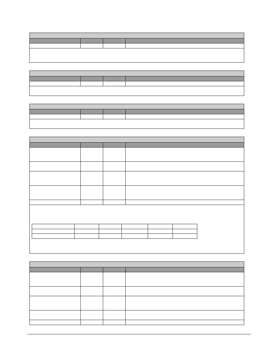
Interrupt Pin - R - 8 bits - [PCI_Reg:3Dh]
Field Name
Bits
Default
Description
Interrupt Pin
7:0
01h
Hard-wired to 01h.
Interrupt Pin Register: This register identifies the interrupt pin a device uses. Since the IDE host controller uses
IRQ14, this value is supposed to be 00. However, the IDE controller will generate the PCI interrupt INTA# signal on
the PCI bus. Therefore, this pin register is set to 01h.
Min_gnt - R - 8 bits - [PCI_Reg:3Eh]
Field Name
Bits
Default
Description
Minimum Grant
7:0
00h
Hard-wired to 0’s and always read as 0’s.
Min_gnt Register: This register specifies the desired settings for how long of a burst the IDE host controller needs
assuming a clock rate of 33MHz. The value specifies a period of time in units of ¼ microseconds.
Max_latency - R - 8 bits - [PCI_Reg:3Fh]
Field Name
Bits
Default
Description
Maximum Latency
7:0
00h
Hard-wired to 0’s and always read as 0’s.
Max_latency Register: This register specifies the Maximum Latency time required before the IDE host controller as
a bus-master can start an accesses.
IDE PIO Timing - RW - 32 bits - [PCI_Reg:40h]
Field Name
Bits
Default
Description
Primary Slave Data
Register Command
Recovery Width
3:0
9h
Slave Data register command recovery width for Primary IDE
bus slave PIO device.
Primary Slave Data
Register Command width
7:4
9h
Slave Data register command width for Primary IDE bus slave
PIO device.
Primary Master Data
Register Command
Recovery Width
11:8
9h
Master Data register command recovery width for primary IDE
bus Master PIO device.
Primary Master Data
Register Command
Width
15:12
9h
Master Data register command width for Primary IDE bus
Master PIO device.
Reserved
31:16
0000h
Reserved. Always read as 0’s
IDE PIO Timing Register: This register controls the IDE interface and selects the timing of the IDE PIO bus-master
cycles.
Note
: Relation of setting value and actual timing of each mode are
PIO Mode
4
3
2
1
0
Command Width
2(90ns)
2(90ns)
3(120ns)
4(150ns)
9(270ns)
Recover Width
0(30ns)
2(90ns)
4(150ns)
7(240ns)
9(270ns)
The above timings are valid and A-Link clock is always 66MHz.
Actual timing is setting value + 1 A-Link clock cycle.
IDE Legacy DMA (Multi-words DMA) Timing Modes - RW - 32 bits - [PCI_Reg:44h]
Field Name
Bits
Default
Description
Primary Slave DMA
Command Recovery
Width
3:0
Fh
Slave DMA command recovery width for Primary IDE bus
Slave DMA device.
Primary Slave DMA
Command Width
7:4
Fh
Slave DMA command width for Primary IDE bus Slave DMA
device.
Primary Master DMA
Command Recovery
Width
11:8
Fh
Master DMA Command recovery width for primary IDE bus
Master DMA device.
Primary Master DMA
Command Width
15:12
Fh
Master DMA Command width for Primary IDE bus Master
DMA device.
Reserved
31:16
0h
Reserved. Always read as 0’s