Scfqctl, system clock control register – Texas Instruments MSP430x4xx User Manual
Page 121
FLL+ Clock Module Registers
4-12
FLL+ Clock Module
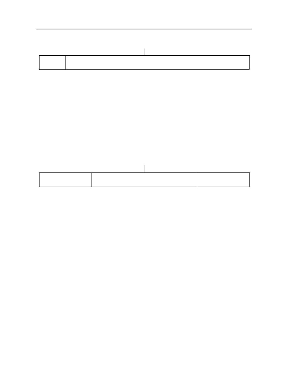
SCFQCTL, System Clock Control Register
7
6
5
4
3
2
1
0
SCFQ_M
N
rw−0
rw−0
rw−0
rw−1
rw−1
rw−1
rw−1
rw−1
SCFQ_M
Bit 7
Modulation. This enables or disables modulation
0
Modulation enabled
1
Modulation disabled
N
Bits
6-0
Multiplier. These bits set the multiplier value for the DCO. N must be > 0 or
unpredictable operation will result.
When DCOPLUS=0: f
DCOCLK
= (N + 1)
⋅
f
crystal
When DCOPLUS=1:
f
DCOCLK
= D x (N + 1)
⋅
f
crystal
SCFI0, System Clock Frequency Integrator Register 0
7
6
5
4
3
2
1
0
FLLDx
FN_x
MODx (LSBs)
rw−0
rw−1
rw−0
rw−0
rw−0
rw−0
rw−0
rw−0
FLLDx
Bits
7-6
FLL+ loop divider. These bits divide f
DCOCLK
in the FLL+ feedback loop.
This results in an additional multiplier for the multiplier bits. See also multi-
plier bits.
00
/1
01
/2
10
/4
11
/8
FN_x
Bits
5-2
DCO Range Control. These bits select the f
DCO
operating range.
0000 0.65 - 6.1 MHz
0001 1.3 - 12.1 MHz
001x 2 - 17.9 MHz
01xx 2.8 - 26.6 MHz
1xxx 4.2 - 46 MHz
MODx
Bits
1−0
Least significant modulator bits. Bit 0 is the modulator LSB. These bits
affect the modulator pattern. All MODx bits are modified automatically by
the FLL+.