IBM uPD78082 User Manual
Page 95
72
CHAPTER 5 CLOCK GENERATOR
Write to OSMS
(MCS
0)
f
XX
Max. 2/f
X
Operating at f
XX
= f
X
/2 (MCS = 0)
Operating at f
XX
= f
X
/2 (MCS = 0)
MCS
Main System Clock Scaler Control
0
1
Scaler used
Scaler not used
0
0
0
0
OSMS
FFF2H
7
6
5
4
3
2
Symbol
1
0
MCS
0
0
Address
After
Reset
R/W
00H
W
0
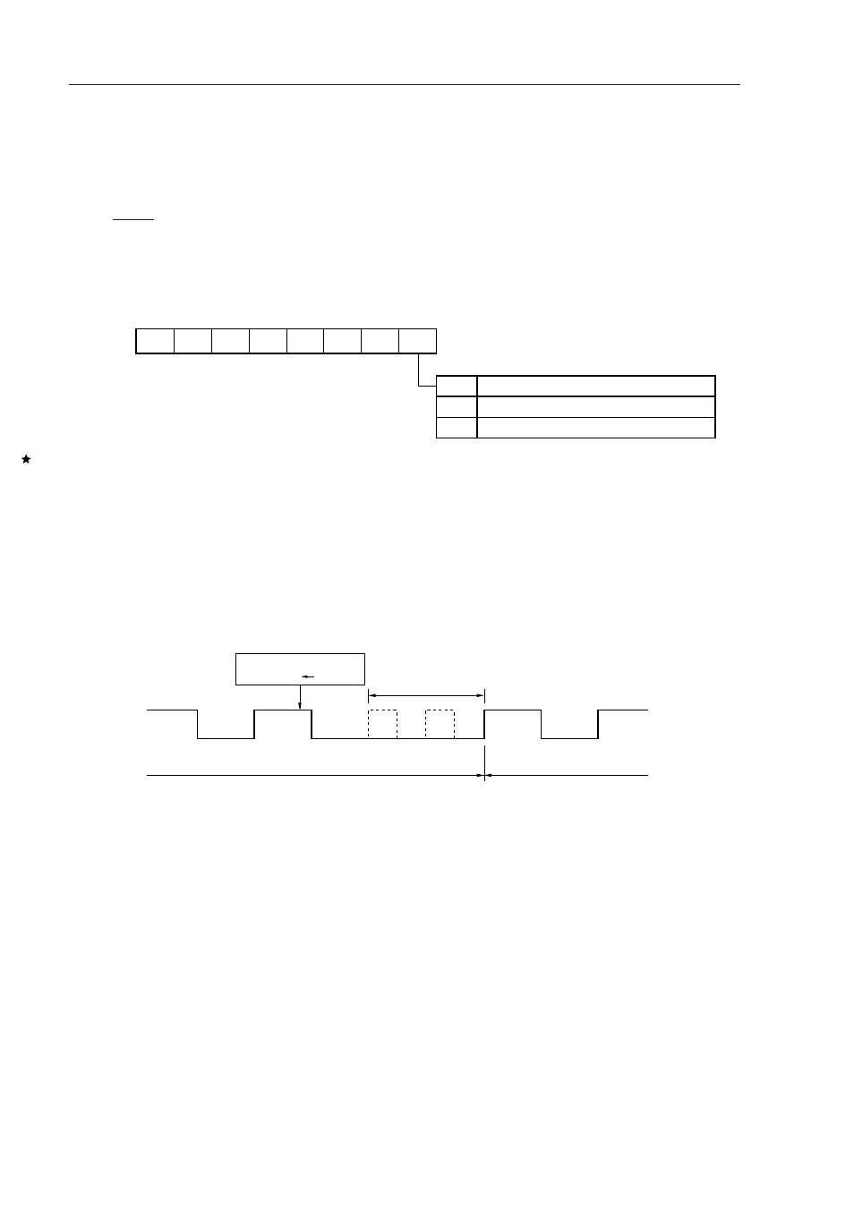
(2) Oscillation mode selection register (OSMS)
This register specifies whether the clock output from the main system clock oscillator without passing through
the scaler is used as the main system clock, or the clock output via the scaler is used as the main system
clock.
OSMS is set with 8-bit memory manipulation instruction.
RESET input sets OSMS to 00H.
Figure 5-3. Oscillation Mode Selection Register Format
Cautions 1. Writing to OSMS should be performed only immediately after reset signal release and before
peripheral hardware operation starts. As shown in Figure 5-4 below, writing data (including
same data as previous) to OSMS cause delay of main system clock cycle up to 2/f
x
during
the write operation. Therefore, if this register is written during the operation, in peripheral
hardware which operates with the main system clock, a temporary error occurs in the count
clock cycle of timer, etc. In addition, because the oscillation mode is changed by this register,
the clocks for peripheral hardware as well as that for the CPU are switched.
Figure 5-4. Main System Clock Waveform due to Writing to OSMS
2. When writing “1” to MCS, V
DD
must be 2.7 V or higher before the write execution.
Remarks f
xx
: Main system clock frequency (fx or fx/2)
f
x
: Main system clock oscillation frequency