3 clock output function control registers – IBM uPD78082 User Manual
Page 136
113
CHAPTER 8 CLOCK OUTPUT CONTROL CIRCUIT
8.3 Clock Output Function Control Registers
The following two types of registers are used to control the clock output function.
• Timer clock select register 0 (TCL0)
• Port mode register 3 (PM3)
(1) Timer clock select register 0 (TCL0)
This register sets PCL output clock.
TCL0 is set with a 1-bit or 8-bit memory manipulation instruction.
RESET input sets TCL0 to 00H.
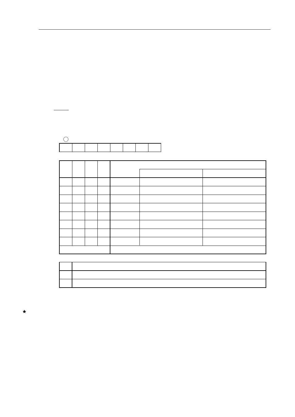
Figure 8-3. Timer Clock Select Register 0 Format
CLOE
7
0
6
0
0
4
TCL03
3
2
1
0
FF40H
Address
TCL0
Symbol
TCL02 TCL01 TCL00
5
00H
After
Reset
R/W
R/W
0
0
0
1
1
1
1
1
Other than above
1
1
1
0
0
0
0
1
0
1
1
0
0
1
1
0
TCL03 TCL02 TCL01
f
XX
f
XX
/2
f
XX
/2
2
f
XX
/2
3
f
XX
/2
4
f
XX
/2
5
f
XX
/2
6
f
XX
/2
7
Setting prohibited
MCS=1
f
X
(5.0 MHz)
f
X
/2 (2.5 MHz)
f
X
/2
2
(1.25 MHz)
f
X
/2
3
(625 kHz)
f
X
/2
4
(313 kHz)
f
X
/2
5
(156 kHz)
f
X
/2
6
(78.1 kHz)
f
X
/2
7
(39.1 kHz)
MCS=0
f
X
/2 (2.5 MHz)
f
X
/2
2
(1.25 MHz)
f
X
/2
3
(625 kHz)
f
X
/2
4
(313 kHz)
f
X
/2
5
(156 kHz)
f
X
/2
6
(78.1 kHz)
f
X
/2
7
(39.1 kHz)
f
X
/2
8
(19.5 kHz)
PCL Output Clock Selection
CLOE
0
1
PCL Output Control
Output disable
Output enable
TCL00
1
0
1
0
1
0
1
0
Cautions 1. When enabling PCL output, set TCL00 to TCL03, then set 1 in CLOE with a 1-bit memory
manipulation instruction.
2. When rewriting TCL0 to other data, stop the clock operation beforehand.
3. Set 0 to bits 4 to 6.
Remarks 1. f
XX
: Main system clock frequency (f
X
or f
X
/2)
2. f
X
: Main system clock oscillation frequency
3. MCS : Oscillation mode selection register (OSMS) bit 0
4. Values in parentheses when operated at f
X
= 5.0 MHz.