IBM uPD78082 User Manual
Page 79
56
CHAPTER 4 PORT FUNCTIONS
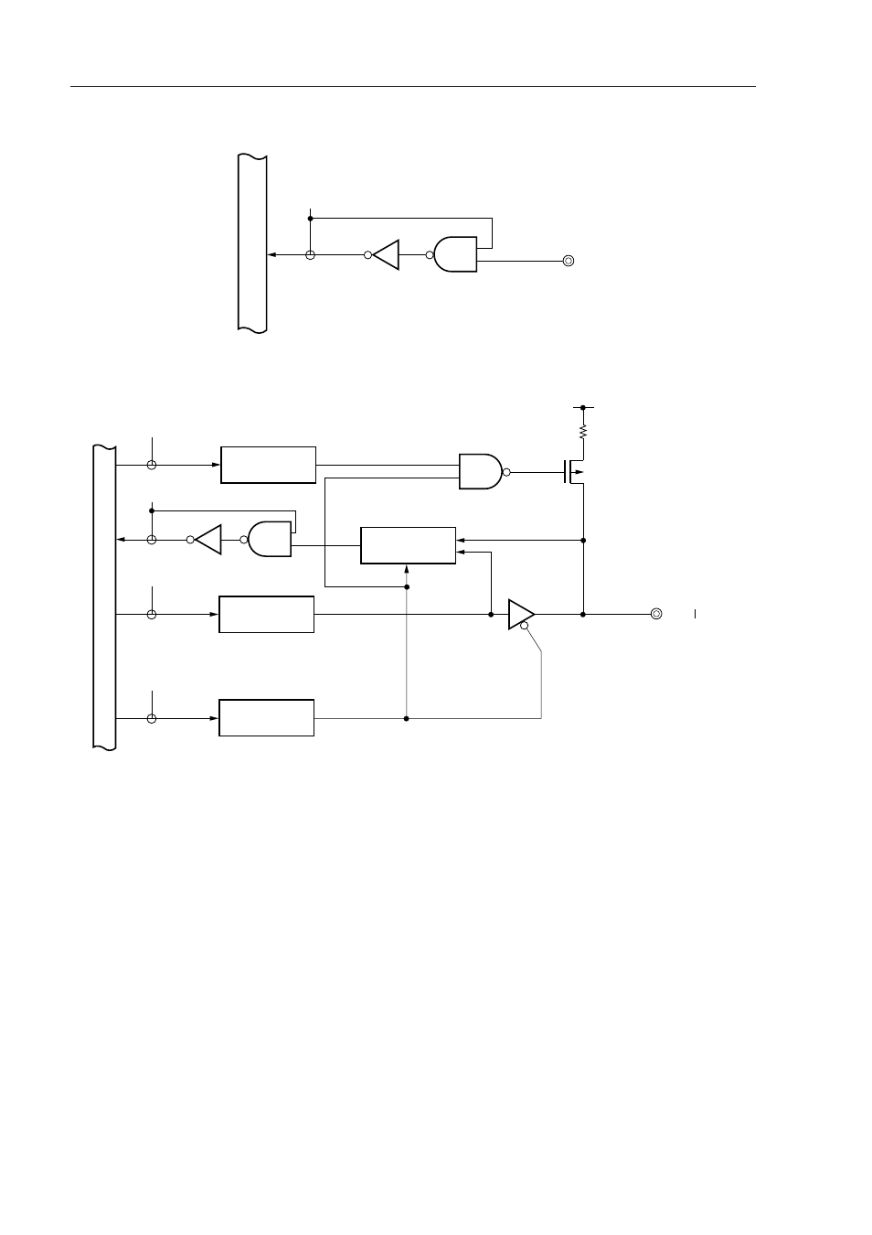
Figure 4-2. P00 Block Diagram
Figure 4-3. P01 to P03 Block Diagram
PUO : Pull-up resistor option register
PM
: Port mode register
RD
: Port 0 read signal
WR : Port 0 write signal
P00
RD
Internal bus
P-ch
WR
PM
WR
PORT
RD
WR
PUO
V
DD
P01/INTP1
P03/INTP3
Selector
PUO0
Output Latch
(P01 to P03)
PM01-PM03
Internal bus
See also other documents in the category IBM Hardware:
- ADSL Bridge/ Router Heritage (167 pages)
- 27L2579 (20 pages)
- DR550 (128 pages)
- LCD/LVDS/LAN (154 pages)
- 22P6959 (50 pages)
- ThinkPad 73P3315 (62 pages)
- ULTRABAY 2000 (62 pages)
- SYSTEM STORAGE DS4000 (38 pages)
- 2257 (252 pages)
- 51 (248 pages)
- 2 (72 pages)
- System Storage N6040 (6 pages)
- 22P6960 (56 pages)
- 07N4108 (11 pages)
- 22P9176 (76 pages)
- 22P6972 (46 pages)
- 48X (60 pages)
- 22P6979 (52 pages)
- 8313 (314 pages)
- 19K4543 (56 pages)
- SC30-3865-04 (513 pages)
- DTLA-305020 (2 pages)
- WebSphere Adapters (226 pages)
- x Series 200 (152 pages)
- Storage Device Enclosure 7214 (4 pages)
- Tivoli and Cisco (516 pages)
- ZSERIES 890 (12 pages)
- 10K0001 (20 pages)
- 31P8128 (112 pages)
- 09N4076 (78 pages)
- Computer Drive (44 pages)
- N7000 (8 pages)
- All-in-One Super7 Single Board Computer PCM-5896 (128 pages)
- 20X (17 pages)
- 73P3309 (64 pages)
- W2H (68 pages)
- 22P6415 (62 pages)
- THINKCENTER 8187 (290 pages)
- NETVISTA 6830/6831 (152 pages)
- 802.11g Wireless Broadband Router WRT-410 (69 pages)
- THINKPAD 72 W DC (70 pages)
- ThinkPad 73P3279 (54 pages)
- HS64 (13 pages)
- THINKVISION MONITOR L150P (35 pages)