8 outline of function – IBM uPD78082 User Manual
Page 35
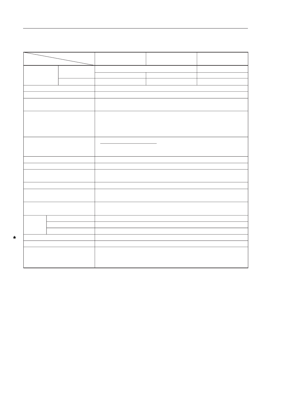
12
CHAPTER 1 OUTLINE
1.8 Outline of Function
Part Number
µ
PD78081
µ
PD78082
µ
PD78083
Item
Internal memory
ROM
Mask ROM
PROM
8 Kbytes
16 Kbytes
24 Kbytes
Note
High-speed RAM
256 bytes
384 bytes
512 bytes
Note
Memory space
64 Kbytes
General register
8 bits
×
32 registers (8 bits
×
8 registers
×
4 banks)
Instruction cycle
Instruction execution time variable function is integrated.
0.4
µ
s/0.8
µ
s/1.6
µ
s/3.2
µ
s/6.4
µ
s/12.8
µ
s (@5.0-MHz operation with main system clock)
Instruction set
• 16-bit operation
• Multiply/divide (8 bits
×
8 bits, 16 bits
÷
8 bits)
• Bit manipulation (set, reset, test, Boolean operation)
• BCD adjust, etc.
I/O ports
Total
: 33
• CMOS input
: 1
• CMOS input/output
: 32
A/D converter
• 8-bit resolution
×
8 channels
Serial interface
• 3-wire serial I/O/UART mode selectable: 1 channel
Timer
• 8-bit timer/event counter: 2 channels
• Watchdog timer: 1 channel
Timer output
2 pins (8-bit PWM output enable)
Clock output
19.5 kHz, 39.1 kHz, 78.1 kHz, 156 kHz, 313 kHz, 625 kHz, 1.25 MHz, 2.5 MHz,
and 5.0 MHz (@ 5.0-MHz operation with main system clock)
Buzzer output
1.2 kHz, 2.4 kHz, 4.9 kHz, and 9.8 kHz
(@ 5.0-MHz operation with main system clock)
Vectored
Maskable
Internal : 8 external : 3
interrupt
Non-maskable
Internal : 1
source
Software
1
Supply voltage
V
DD
= 1.8 to 5.5 V
Operating ambient temperature
T
A
= –40 to +85
°
C
Package
• 42-pin plastic shrink DIP (600 mil)
• 44-pin plastic QFP (10
×
10 mm)
• 42-pin ceramic shrink DIP (with window) (600 mil) (
µ
PD78P083 only)
Note
Internal PROM and high-speed RAM capacities can be changed by setting the internal memory size
switching register (IMS).