2 prom programming mode pins ( upd78p083 only) – IBM uPD78082 User Manual
Page 39
16
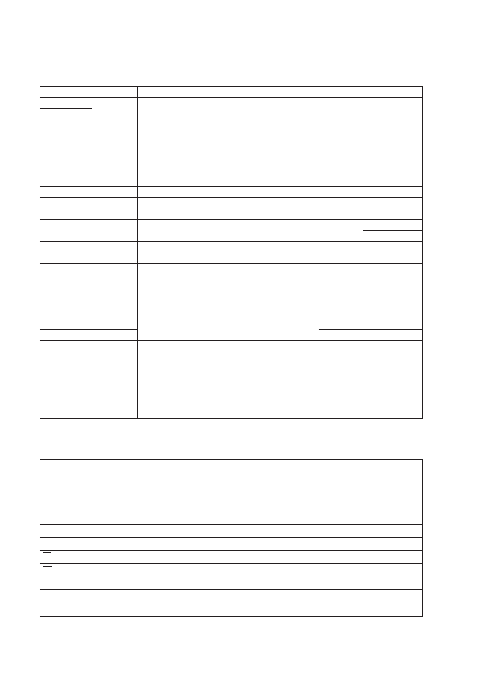
CHAPTER 2 PIN FUNCTION
Pin Name
Input/Output
Function
After Reset
Alternate Function
INTP1
Input
External interrupt request input by which the active edge
Input
P01
INTP2
(rising edge, falling edge, or both rising and falling edges)
P02
INTP3
can be specified.
P03
SI2
Input
Serial interface serial data input.
Input
P70/RxD
SO2
Output
Serial interface serial data output.
Input
P71/TxD
SCK2
Input/output
Serial interface serial clock input/output.
Input
P72/ASCK
RxD
Input
Asynchronous serial interface serial data input.
Input
P70/SI2
TxD
Output
Asynchronous serial interface serial data output.
Input
P71/SO2
ASCK
Input
Asynchronous serial interface serial clock input.
Input
P72/SCK2
TI5
Input
External count clock input to 8-bit timer (TM5).
Input
P100/TO5
TI6
External count clock input to 8-bit timer (TM6).
P101/TO6
TO5
Output
8-bit timer output. (also used for 8-bit PWM output)
Input
P100/TI5
TO6
P101/TI6
PCL
Output
Clock output. (for main system clock trimming)
Input
P35
BUZ
Output
Buzzer output.
Input
P36
ANI0-ANI7
Input
A/D converter analog input.
Input
P10-P17
AV
REF
Input
A/D converter reference voltage input.
–
–
AV
DD
–
A/D converter analog power supply. Connected to V
DD
.
–
–
AV
SS
–
A/D converter ground potential. Connected to V
SS
.
–
–
RESET
Input
System reset input.
–
–
X1
Input
Main system clock oscillation crystal connection.
–
–
X2
–
–
–
V
DD
–
Positive power supply.
–
–
V
PP
–
High-voltage applied during program write/verification.
–
–
Connected directly to V
SS
in normal operating mode.
V
SS
–
Ground potential.
–
–
IC
–
Internal connection. Connect directly to V
SS
.
–
–
NC
–
Does not internally connected. Connect to V
SS
.
–
–
(It can be left open)
(2) Pins other than port pins
2.1.2 PROM programming mode pins (
µ
PD78P083 only)
Pin Name
Input/Output
Function
RESET
Input
PROM programming mode setting.
When +5 V or +12.5 V is applied to the V
PP
pin or a low level voltage is applied to the
RESET pin, the PROM programming mode is set.
V
PP
Input
High-voltage application for PROM programming mode setting and program write/verify.
A0 to A14
Input
Address bus
D0 to D7
Input/output
Data bus
CE
Input
PROM enable input/program pulse input
OE
Input
Read strobe input to PROM
PGM
Input
Program/program inhibit input in PROM programming mode
V
DD
—
Positive power supply
V
SS
—
Ground potential