IBM uPD78082 User Manual
Page 165
142
CHAPTER 11 SERIAL INTERFACE CHANNEL 2
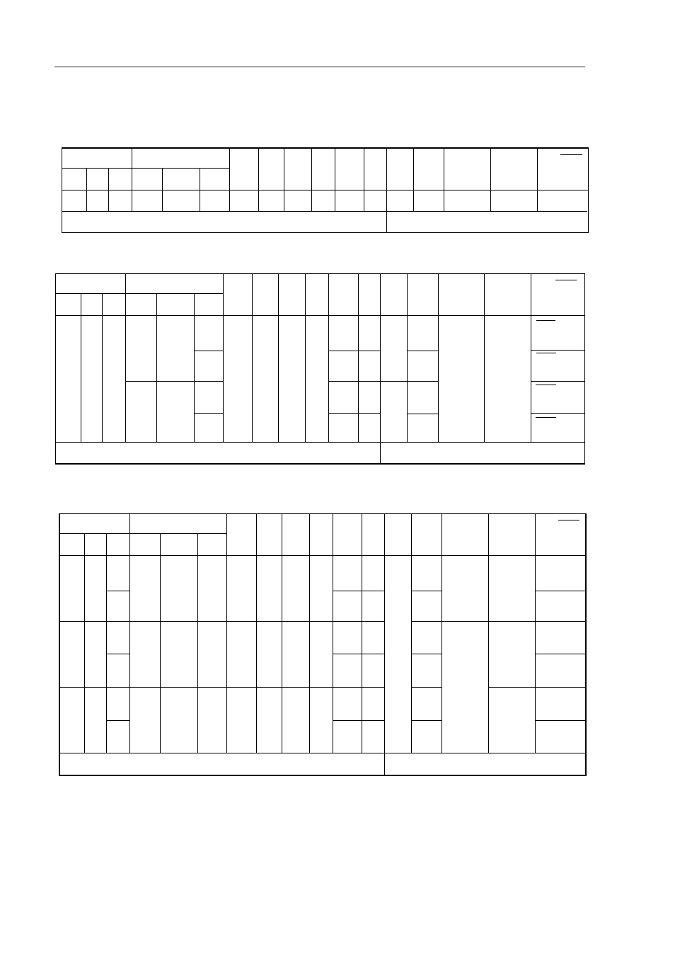
Table 11-2. Serial Interface Channel 2 Operating Mode Settings
(1) Operation Stop Mode
(2) 3-wire Serial I/O Mode
(3) Asynchronous Serial Interface Mode
Notes 1. Can be used freely as port function.
2. Can be used as P70 (CMOS input/output) when only transmitter is used.
Remark
×
: Don’t care
PM
××
: Port mode register
P
××
: Port output latch
P72/SCK2
/ASCK Pin
Functions
P71/SO2
/TxD Pin
Functions
P70/SI2
/RxD Pin
Functions
Shift
Clock
Start
Bit
TXE RXE SCK CSIE2 CSIM22 CSCK
PM70 P70 PM71 P71 PM72 P72
ASIM
CSIM2
0
0
x
0
x
x
x
Note1
x
Note1
x
Note1
x
Note1
x
Note1
x
Note1
—
—
P70
P71
P72
Other than above
Setting prohibited
P72/SCK2
/ASCK Pin
Functions
P71/SO2
/TxD Pin
Functions
P70/SI2
/RxD Pin
Functions
Shift
Clock
Start
Bit
TXE RXE SCK CSIE2 CSIM22 CSCK
PM70 P70 PM71 P71 PM72 P72
ASIM
CSIM2
0
0
0
1
1
0
1
0
1
0
1
1
Note2
x
Note2
0
1
1
0
1
0
x
1
x
1
MSB
LSB
External
clock
Internal
clock
External
clock
Internal
clock
SI2
SO2
(CMOS
output)
SCK2 input
SCK2 output
SCK2 input
SCK2 output
Other than above
Setting prohibited
Note2
P72/SCK2
/ASCK Pin
Functions
P71/SO2
/TxD Pin
Functions
P70/SI2
/RxD Pin
Functions
Shift
Clock
Start
Bit
TXE RXE SCK CSIE2 CSIM22 CSCK
PM70 P70 PM71 P71 PM72 P72
ASIM
CSIM2
1
0
1
0
1
1
0
0
0
0
0
0
0
0
0
0
x
Note1
x
Note1
0
1
1
1
x
x
LSB
External
clock
Internal
clock
External
clock
Internal
clock
External
clock
Internal
clock
P70
TxD
(CMOS
output)
ASCK input
P72
ASCK input
P72
ASCK input
P72
P71
Note1
x
Note1
x
1
0
1
0
1
1
1
x
x
x
Note1
Note1
x
RxD
Note1
x
Note1
x
0
1
1
x
TxD
(CMOS
output)
Note1
x
Note1
x
Other than above
Setting prohibited