Triac output – Echelon FT 3150 Smart Transceiver User Manual
Page 92
Chapter 3 - Input/Output Interfaces
86
FT 3120 / FT 3150 Smart Transceiver Data Book
Triac Output
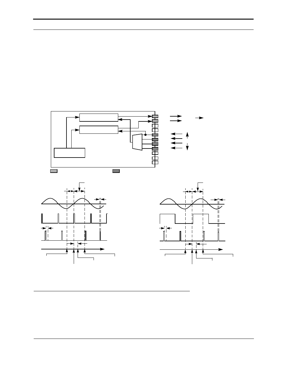
On the FT Smart Transceiver, a timer/counter may be configured to control the delay of an output signal with respect
to a synchronization input. This synchronization can occur on the rising edge, the falling edge, or both the rising and
falling edges of the input signal. For control of AC circuits using a triac device, the sync input is typically a zero-
crossing signal, and the pulse output is the triac trigger signal. Table 3.6 shows the resolution and maximum range of
the delay. See Figure 3.49.
The output gate pulse is gated by an internal clock with a constant period of 25.6 µs (independent of the FT Smart
Transceiver input clock). Since the input trigger signal (zero crossing) is asynchronous relative to this internal
clock, there is a jitter, t
jit
, associated with the output gate pulse.
The actual active edge of the sync input and the triac gate output can be set by using the clock edge or invert
parameters, respectively.
Figure 3.49 Triac Output Latency Values
trigger
output
System Clock
Divide Chain
Timer/Counter 1
Timer/Counter 2
sync
IO10
IO9
IO8
IO0
IO1
IO2
IO3
IO4
IO5
IO6
IO7
mux
to
triac
gate
from
zero
crossing
detector
t
ret
END OF
io_out()
t
gpw
NEW
GATE-PULSE
DELAY
t
fout
FIRST GATE
PULSE WITH
NEW DELAY
HARDWARE
UPDATED
START
OF
io_out()
TIME
TRIAC GATE
(OUTPUT)
ZERO
CROSSING
DETECTOR
AC
INPUT
CLOCK EDGE
(+) or (-)
t
ret
END OF
io_out()
t
gpw
NEW
GATE-PULSE
DELAY
t
fout
FIRST GATE
PULSE WITH
NEW DELAY
HARDWARE
UPDATED
START
OF
io_out()
TIME
TRIAC GATE
(OUTPUT)
ZERO
CROSSING
DETECTOR
AC
INPUT
CLOCK EDGE
(+-)
High Current Sink Drivers
t
jit
t
jit
Optional Pull-Up Resistors