Echelon FT 3150 Smart Transceiver User Manual
Page 17

FT 3120 / FT 3150 Smart Transceiver Data Book
11
Neuron Processor Architecture
addresses for CALL instructions, and may also be used for temporary data storage. This stack architecture leads to
very compact code. Tables 2.3, 2.42.4, and 2.5 outline the instruction set.
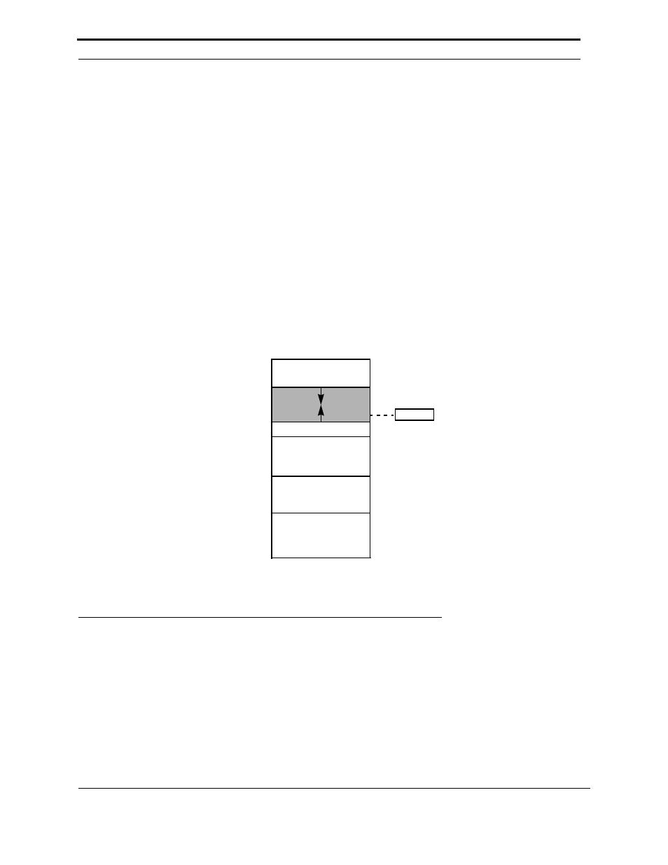
Figure 2.4 shows the layout of a base page, which may be up to 256 bytes long. Each of the three processors uses a
different base page, whose address is given by the contents of the BP register of that processor. The top of the data
stack is in the 8-bit TOS register, and the next element in the data stack is at the location within the base page at the
offset given by the contents of the DSP register. The data stack grows from low memory towards high memory. The
assembler shorthand symbol NEXT refers to the contents of the location (BP+DSP) in memory, which is not an actual
processor register.
Pushing a byte of data onto the data stack involves the following steps: incrementing the DSP register, storing the
current contents of TOS at the address (BP+DSP) in memory, and moving the byte of data to TOS.
Popping a byte of data from the data stack involves the following steps: moving TOS to the destination, moving the
contents of the address (BP+DSP) in memory to TOS, and decrementing the DSP register.
The return stack grows from high memory towards low memory. Executing a subroutine call involves the following
steps: storing the high byte of the instruction pointer register IP at the address (BP+RSP) in memory, decrementing
RSP, storing the low byte of IP at the address (BP+RSP) in memory, decrementing RSP, and moving the destination
address to the IP register.
Similarly, returning from a subroutine involves the following steps: incrementing RSP, moving the contents of
(BP+RSP) to the low byte of the IP register, incrementing RSP, and moving the contents of (BP+RSP) to the high
byte of IP.
Figure 2.4 Base Page Memory Layout
A processor instruction cycle is three system clock cycles, or six input clock (CLK1) cycles. Most instructions take
between one and seven processor instruction cycles. At an input clock rate of 40MHz, instruction times vary between
0.15
µs and 1.05 µs. Execution time scales inversely with the input clock rate. The formula for instruction time is:
Tables 2.3, 2.42.4, and 2.5 list the processor instructions, their timings (in cycles) and sizes (in bytes). This is
provided for purposes of calculating the execution time and size of code sequences. All programming of the FT Smart
Transceiver is done with Neuron C using a LonBuilder or NodeBuilder development tool. The Neuron C compiler
can optionally produce an assembly listing, and examining this listing can help the programmer to optimize his/her
Neuron C source code.
BP*
BP+0x8
BP+0x7
BP+0x18
BP+0x17
BP+DSP
BP+RSP
Data Stack
Return Stack
Sixteen Byte Registers
Four 16-bit
Pointer Registers
TOS
*BP = Base Page.
NEXT
