Echelon FT 3150 Smart Transceiver User Manual
Page 16
Chapter 2 - Hardware Resources
10
FT 3120 / FT 3150 Smart Transceiver Data Book
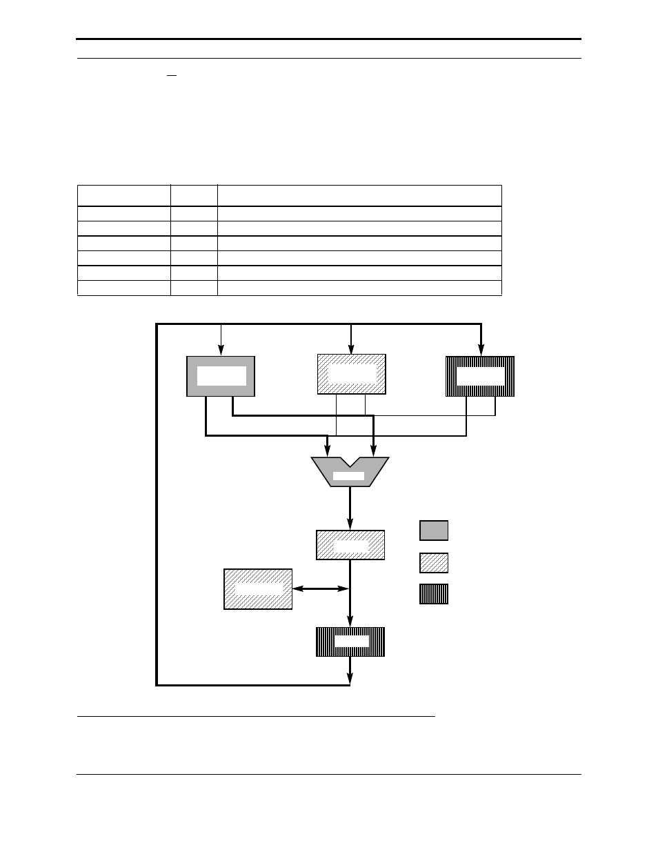
address, data, and R/W signals are reflected on the corresponding external lines when utilized by any of the internal
processors. Each CPU minor cycle consists of three system clock cycles, or phases; each system clock cycle is two
input clock cycles. The minor cycles of the three processors are offset from one another by one system clock cycle, so
that each processor can access memory and ALUs once during each instruction cycle. Figure 2.3 shows the active
elements for each processor during one of the three phases of a minor cycle. Therefore, the system pipelines the three
processors, reducing hardware requirements without affecting performance. This allows the execution of three
processes in parallel without time-consuming interrupts and context switching.
Table 2.2 Register Set
Figure 2.3 Processor/Memory Activity During One of the Three System Clock Cycles of a Minor Cycle
The architecture is stack-oriented; one 8-bit wide stack is used for data references, and the ALU operates on the TOS
(Top of Stack) register and the next entry in the data stack which is in RAM. A second stack stores the return
Mnemonic
Bits
Contents
FLAGS
8
CPU Number, Fast I/O Select, and Carry Bit
IP
16
Next Instruction Pointer
BP
16
Address of 256-Byte Base Page
DSP
8
Data Stack Pointer Within Base Page
RSP
8
Return Stack Pointer Within Base Page
TOS
8
Top of Data Stack, ALU Input
Active elements – Processor 1
Active elements – Processor 2
Active elements – Processor 3
Processor 1
Registers
ALUs
Latch
Memory
Latch
Processor 3
Registers
Processor 2
Registers