Power supply, ground, and noise considerations – Echelon FT 3150 Smart Transceiver User Manual
Page 136
Appendix C - Design and Handling Guidelines
130
FT 3120 / FT 3150 Smart Transceiver Data Book
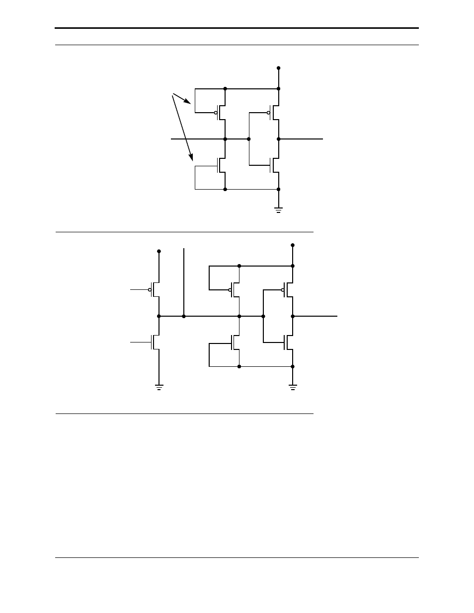
Figure C.2 Digital Input
Figure C.3 Digital I/O
Power Supply, Ground, and Noise Considerations
The most important considerations for PCB layout deal with noise. This includes noise on the power supply, noise
generated by the digital circuitry on the device, and coupling digital signals into the analog signals. The best PCB
layout methods to prevent noise induced problems are the following:
•
Keep digital signals as far away from analog signals as possible.
•
Use short, low-inductance traces for the analog circuitry to reduce inductive, capacitive, and radio frequency
noise sensitivities.
•
Use short, low-inductance traces for the digital circuitry to reduce inductive, capacitive, and radio frequency
radiated noise.
INPUT BUFFER
V
DD
P
N
PIN
PROTECTION
ESD
INPUT BUFFER
V
DD
P
N
PIN
V
DD
P
N
OUTPUT
BUFFER