Echelon FT 3150 Smart Transceiver User Manual
Page 15
FT 3120 / FT 3150 Smart Transceiver Data Book
9
Neuron Processor Architecture
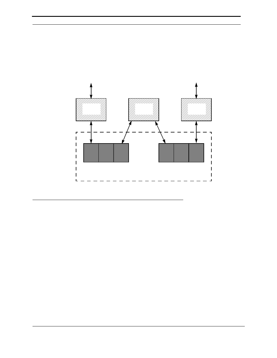
Processor 2 is the network processor that implements layers 3 through 6 of the LonTalk protocol stack. It handles
network variable processing, addressing, transaction processing, authentication, background diagnostics, software
timers, network management, and routing functions. Processor 2 uses network buffers in shared memory to
communicate with Processor 1, and application buffers to communicate with Processor 3. These buffers are also
located in shared RAM memory. Access to them is mediated with hardware semaphores to resolve contention when
updating shared data.
.
Figure 2.2 Processor Organization Memory Allocation
Processor 3 is the application processor. It executes the code written by the user, together with the operating system
services called by user code. The primary programming language used by applications is Neuron C, a derivative of
the ANSI C language optimized and enhanced for L
ON
W
ORKS
distributed control applications. The major
enhancements are the following (see the Neuron C Programmer’s Guide for details):
•
A network communication model, based on functional blocks and network variables, that simplifies and pro-
motes data sharing between like and disparate devices.
•
A network configuration model, based on functional blocks and configuration properties, that facilitates
interoperable network configuration tools.
•
A type model based on standard and user resource files that expands the market for interoperable devices by
simplifying the integration of devices from multiple manufacturers.
•
An extensive set of I/O drivers that support the I/O capabilities of the Neuron core.
•
Powerful event driven programming extensions that provide easy handling of network, I/O, and timer
events.
The support for all these capabilities is part of the Neuron firmware, and does not need to be written by the
programmer.
Each of the three identical processors has its own register set (Table 2.2), but all three processors share data, ALUs
(arithmetic logic units) and memory access circuitry (Figure 2.3). On the FT 3150 Smart Transceiver, the internal
Shared
Communications
Port
Input/Output
Application Buffers
Network Buffers
Applica-
tion
Network
Proces-
MAC
Proces-