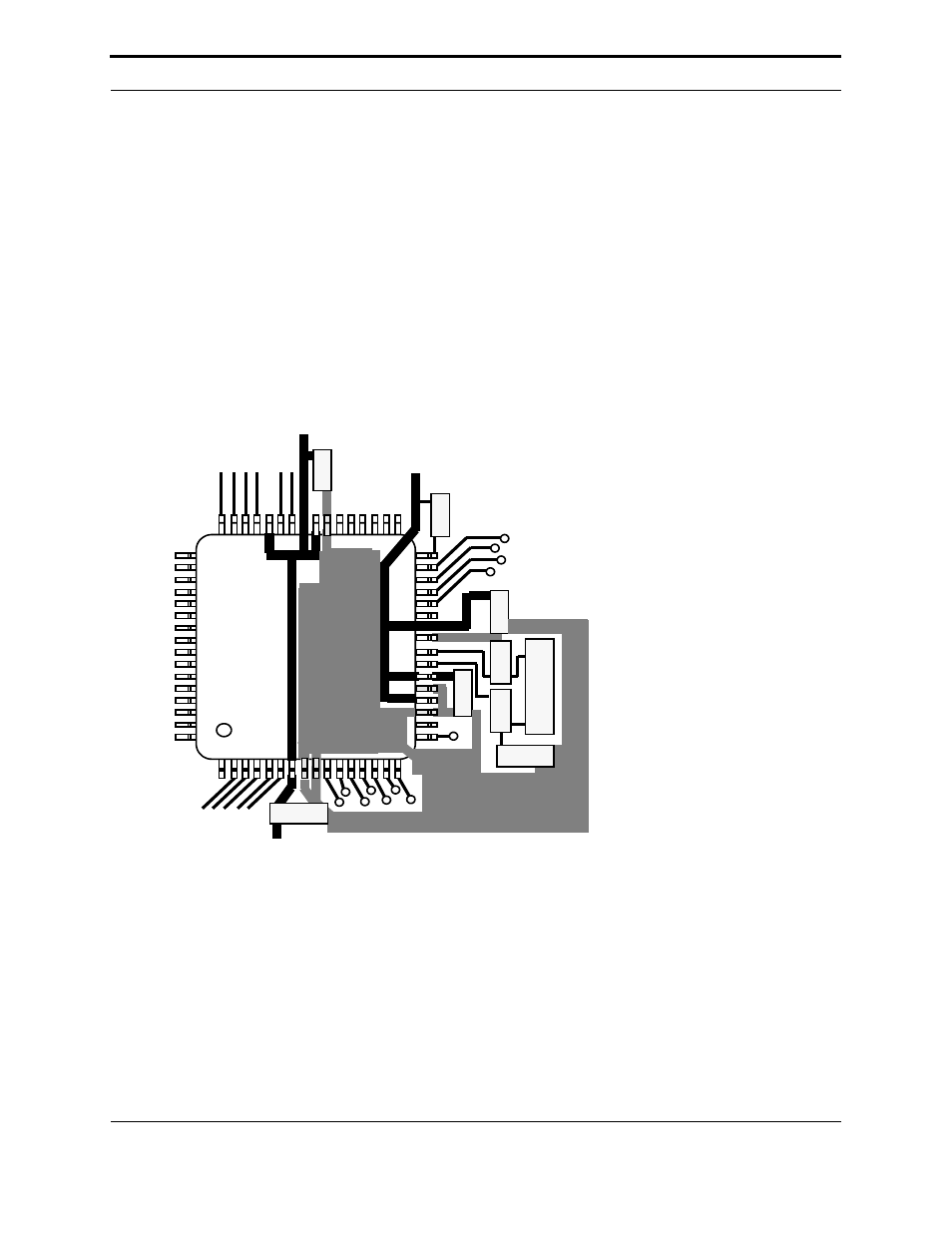
Recommended bypass capacitor placement – Echelon FT 3150 Smart Transceiver User Manual
Page 144

Appendix C - Design and Handling Guidelines
138
FT 3120 / FT 3150 Smart Transceiver Data Book
Recommended Bypass Capacitor Placement
Proper decoupling is required to ensure proper operation of an FT Smart Transceiver. When connecting V
DD
decoupling capacitors to FT Smart Transceivers, make the leads as short as possible. All V
DD
pins must be tied to
+5V, and all V
SS
pins to ground. Keep the crystal circuit close to the FT Smart Transceiver and isolated from
communication lines.
Bypass capacitors should be 0.1µF or 0.33µF ceramic or dipped-mica capacitors and should be placed as close to
V
DD
pins as possible. V
DD
and GND loops should be avoided. Minimum recommended configurations are:
•
FT 3150 Smart Transceiver: 0.1µF bypass capacitor between pins: 7:8, 21:22, 25:26, 39:40.
•
FT 3120 Smart Transceiver: 0.1µF bypass capacitor between pins: 10:11, 12:13, 16:18, 31:32.
The following figures, Figure C.9, Figure C.10 and Figure C.11, show suggested bypass capacitor placement and
crystal circuit trace outlines.
KEY LAYOUT RULES
1. If possible, use 4-layer (or more) boards. This would greatly simplify the layout and reduce grounding and noise-related problems.
2. For 2-layer boards, the four bypass capacitors must be close to the FT Smart Transceiver IC. V
DD
and ground must be large traces to reduce
inductance and noise.
3. The crystal must be isolated from any digital signal. If clock 2 is being used for other circuit signals, keep the trace short or buffer it. The
added board capacitance and input capacitance of other devices being driven will skew the crystal frequency.
4. On 2-layer boards, avoid running high-frequency digital signal traces under crystal circuit or input pins of the communications signals, on
opposite sides of the board.
5. Ensure that power supply and ground traces are large enough to handle the peak surge switching currents. Otherwise there will be power
supply dips on the V
DD
pins, which may cause errors in the checksum calculation, resulting in the FT Smart Transceiver going applicationless.
NOTE:
C = Capacitor, surface mount.
R = Resistor.
X = Crystal.
21
25
1
8
39
C
C
C
R
C
X
C
R
C
FT 3150 SMART TRANSCEIVER 64-LEAD TQFP
