Echelon FT 3150 Smart Transceiver User Manual
Page 141
FT 3120 / FT 3150 Smart Transceiver Data Book
135
Handling Precautions and Electrostatic Discharge
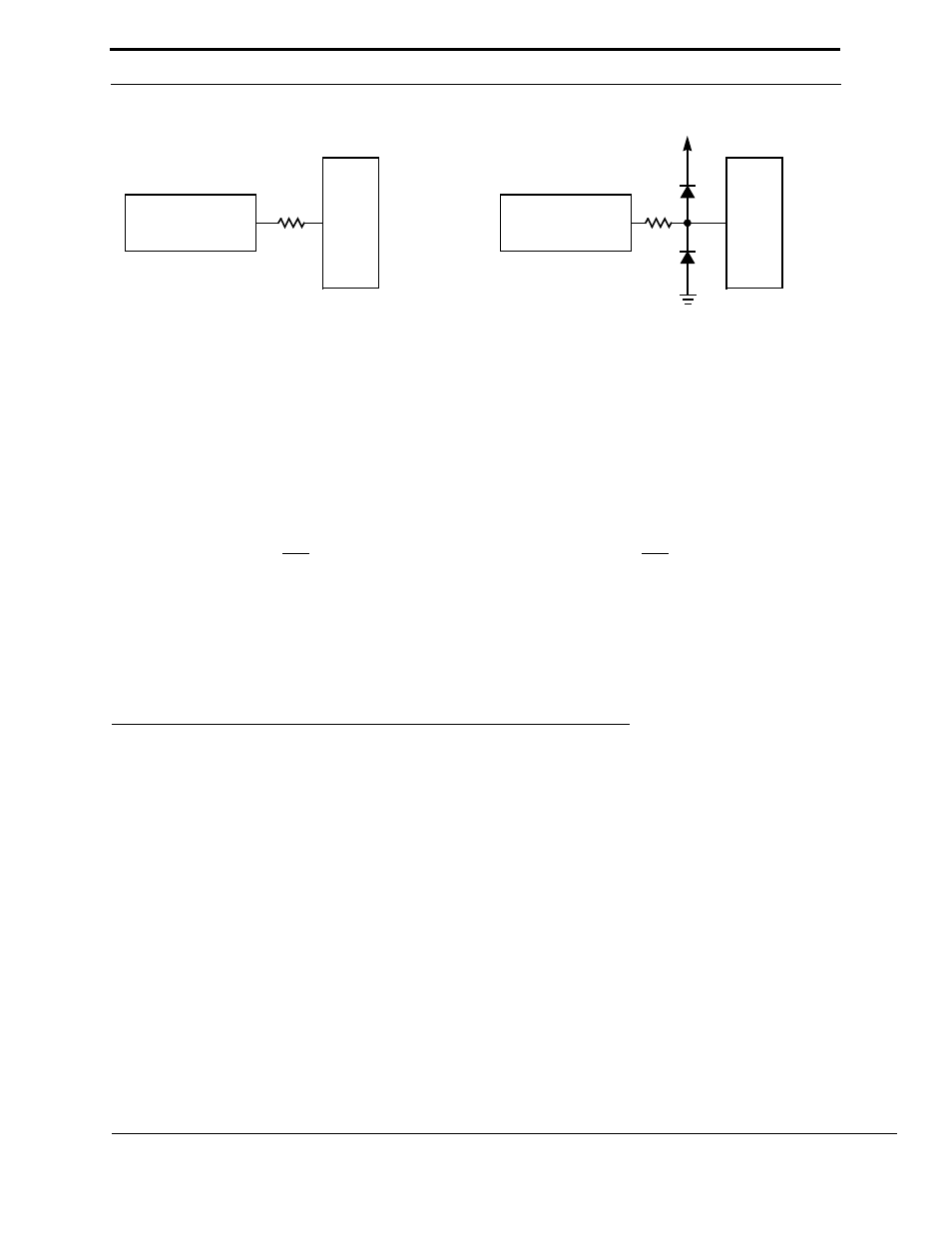
Figure C.6 Networks for Minimizing ESD and Reducing CMOS Latch-Up Susceptibility
t
C
•k
R
≈
V
DD
V
SS
R1
R2
TO OFF-BOARD
CONNECTION
TO OFF-BOARD
CONNECTION
MOS
INPUT
OR
OUTPUT
MOS
INPUT
OR
OUTPUT
Advantage: Requires minimal board area.
Disadvantage:R1 > R2 for the same level of
protection, therefore rise and fall
times, propagation delays, and
output drives are severely affected.
D1
D2
Advantage: R2 < R1 for the same level of
protection. Impact on ac and dc
characteristics is minimized.
Disadvantage: More board area, higher initial cost.
NOTE: These networks are useful for protecting the following:
a.digital inputs and outputs
b.analog inputs and outputs
c.three-state outputs
d.bidirectional (I/O) ports
Equation 1 – Propagation Delay vs. Se-
ries Resistance
where:
R = the maximum allowable series resistance in ohms
t = the maximum tolerable propagation delay in seconds
C = the board capacitance plus the input capacitance
of the driven device in farads
k = 0.33 for the TTL input levels (switch point = 1.3 V)
Equation 2 – Rise Time vs.
Series Resistance
t
C
•k
R
≈
where:
R = the maximum allowable series resistance in ohms
t = the maximum rise time per data sheet in seconds
C = the board capacitance plus the input capacitance
of the driven device in farads
k = 2.3 for other devices