Pc board layout guidelines, Tx rx – Echelon FT 3150 Smart Transceiver User Manual
Page 101
FT 3120 / FT 3150 Smart Transceiver Data Book
95
PC Board Layout Guidelines
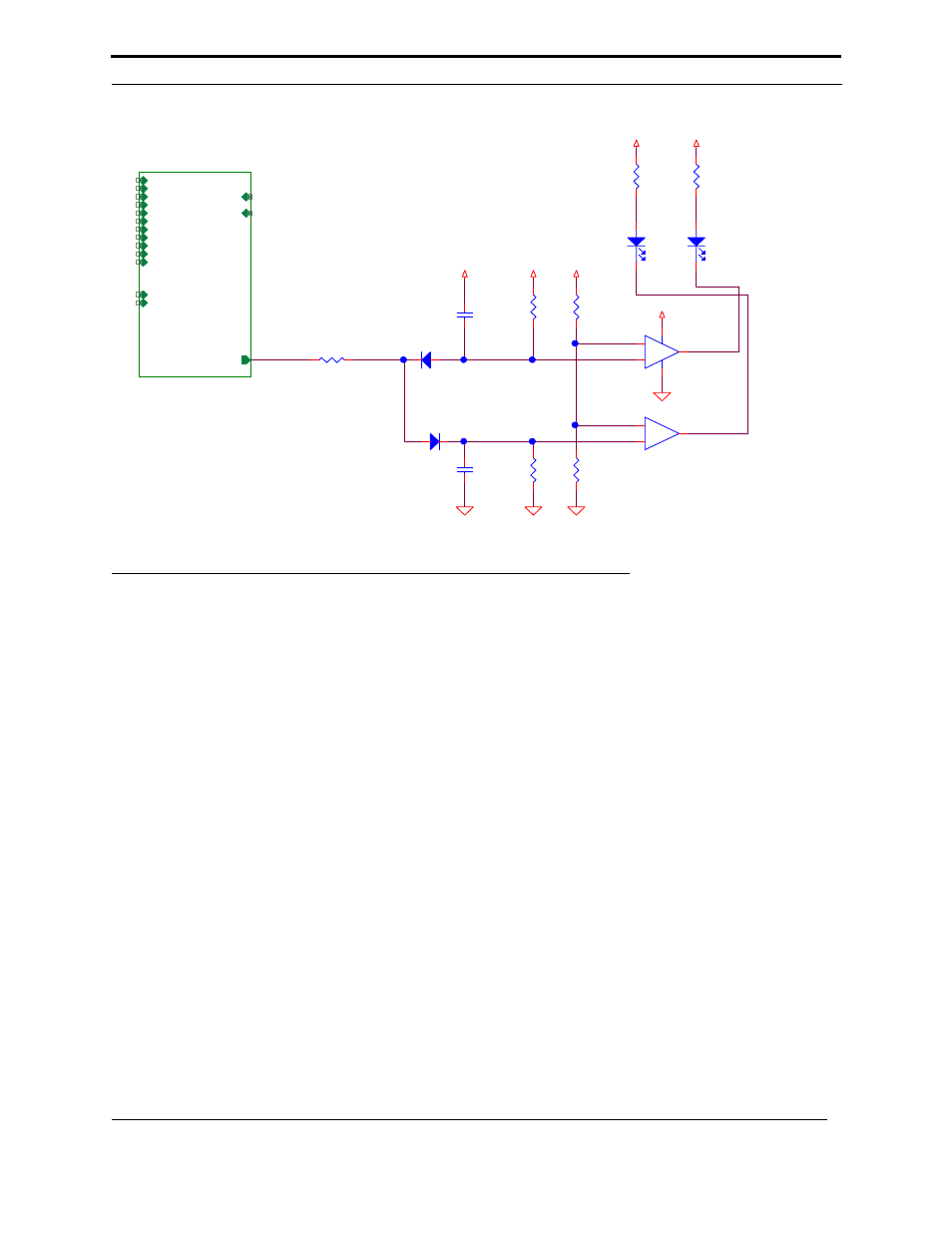
Figure 4.2 Optional COMM_ACTIVE LED Drive Circuit
The example COMM_ACTIVE LED drive circuit shown in Figure 4.2 is for interfacing the FT 3120 or FT 3150
Smart Transceiver COMM_ACTIVE pin to LEDs. These TX and RX activity LEDs can be used to provide visual
indication of physical transceiver activity. The circuit shown in the figure is from the schematic for Echelon’s FT
Mini EVK Evaluation Kit boards. The full schematics for these boards are included on the CD-ROM that ships
with the evaluation kit.
The COMM_ACTIVE pin is normally in a high-impedance state, but it is driven high by the Smart Transceiver
chip for the duration of a transmitted packet. Also, it is driven low for the duration of a received packet. Note that
the COMM_ACTIVE pin is driven low during the reception of a packet from the network, regardless of whether
that packet is addressed to the device, and regardless of whether the packet has a valid CRC (which cannot be
checked until the entire packet is received).
The example circuit shown in Figure 4.2 uses TLC372 comparators to detect whether the COMM_ACTIVE pin is
high, low, or in the middle high-impedance state. The outputs of the comparators are used to drive the appropriate
TX/RX LEDs. The time constants provided by C209, C210, R216, and R217 help to stretch the packet activity
signals out in time to provide more visible LED flashes.
Electrical and mechanical specifications for the FT Smart Transceivers and the pin number for the
COMM_ACTIVE signal are documented in the FT 3120 and FT 3150 Smart Transceiver Datasheet.
PC Board Layout Guidelines
An example of a PC board layout using the through-hole FT-X1 transformer is shown in Figure 4.3. For an example
of a PCB layout using the surface mount (SMT) FT-X2 transformer, refer to Appendix D. The scale of figure 4.3 is
approximately 4X, but it is not intended for use as finished PCB artwork. Variations on this suggested PCB layout
FT_CA
C209
0.1uF
0603
16V
X7R
10%
1
2
D216A
BAV99
SOT-23
1
3
D217B
BAV99
SOT-23
3
2
R216
24.9K
0603
1%
1
2
FT_CAR
LED202
LED
GREEN
2
1
LED201
LED
GREEN
2
1
R217
24.9K
0603
1%
1
2
R218
100K
0603
1%
1
2
R219
100K
0603
1%
1
2
+
-
V+
V-
U204A
TLC372
TSSOP-8
3
2
1
8
4
+
-
U205B
TLC372
TSSOP-8
5
6
7
R215
1.00K
0603
1%
1
2
TX
RX
VDD5
VDD5
C210
0.1uF
0603
16V
X7R
10%
1
2
VDD5
VDD5
P2V5
P2V5
FT_RXS
FT-3120_CORE
FT-3120_CORE
IO0
IO1
IO2
IO3
IO4
IO5
IO6
IO7
IO8
IO9
IO10
SVC-
RST-
COMM_ACTIVE
NETA
NETB
TX-
RX-
RX-
R202
1.00K
0603
1%
1
2
FT_TXS
R201
1.00K
0603
1%
1
2
VDD5
TX-
VDD5