Echelon FT 3150 Smart Transceiver User Manual
Page 71
FT 3120 / FT 3150 Smart Transceiver Data Book
65
Serial I/O Objects
the active edge of the clock to negative. One of the IO0 – IO7 pins may be designated as a timeout pin. A logic 1
level on the timeout pin causes the Neurowire slave I/O operation to be terminated before the specified number of bits
has been transferred. This prevents the FT Smart Transceiver watchdog timer from resetting the chip in the event that
fewer than the requested number of bits are transferred by the external clock. See Figure 3.30.
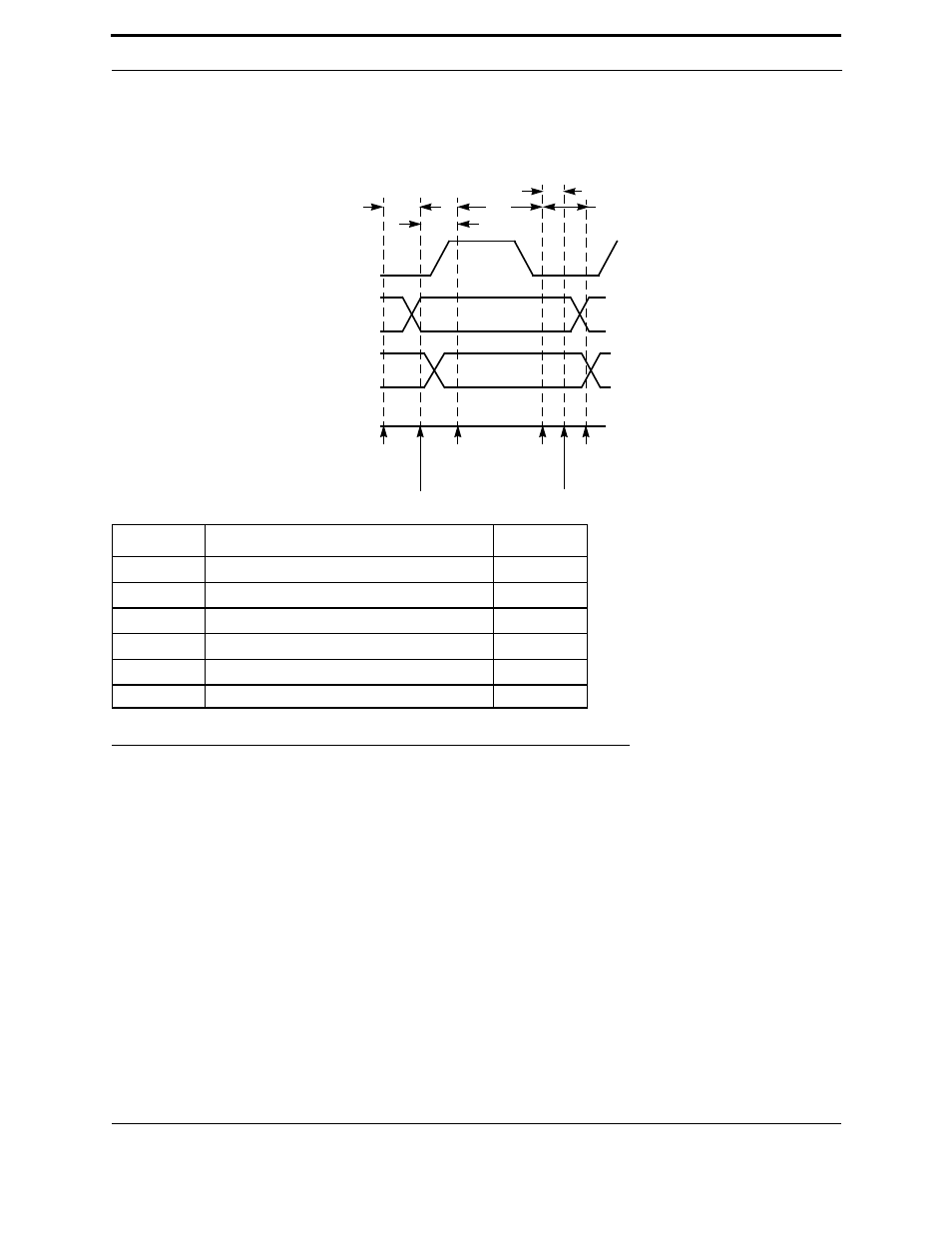
Figure 3.30 Neurowire (SPI) Slave Timing
The algorithm for each bit of output/input for the Neurowire slave objects is described below. In this description, the
default active clock edge (positive) is assumed; if the invert keyword is used, all clock levels stated should be
reversed.
1.
Set IO9 to the next output bit value.
2.
Test pin IO8, the clock input, for a high level. This is the test for the rising edge of the input clock. If the input
clock is still low, sample the timeout event pin and abort if high.
3.
When the input clock is high, store the next data input bit as sampled on pin IO10.
4.
Test the input clock for a low input level. This is the test for the falling edge of the input clock. If the input clock
is still high, sample the timeout event pin and abort if high.
5.
When the input clock is low, return to step 1 if there are more bits to be processed.
6.
Else return the number of bits processed.
When either clock input test fails (that is, the clock is sampled before the next transition), there is an additional
timeout check time of 19.8 µs (wait for clock high) or 19.2 µs (wait for clock low) added to that stage of the
algorithm.
Parameter
Description
Typ
t
fin
Function call to data bit out
41.4 µs
t
ret
Return from function
19.2 µs
t
docki
Data out to input clock and data sampled
4.8 µs
t
cklo
Data sampled to clock low sampled
24.0 µs
t
cklodo
Clock low sampled to data output
25.8 µs
f
Clock frequency (max)
18.31 kHz
t
fin
DATA OUT
DATA IN
INPUT
CLOCK
TIME
t
ret
t
cklo
t
cklodo
START
OF
io_in()
END OF
io_in()
DATA
OUTPUT
CLOCK AND
DATA
SAMPLED
DATA
OUTPUT
CLOCK
SAMPLED
t
docki