Campbell Scientific CR23X Micrologger User Manual
Page 80
SECTION 6. 9-PIN SERIAL INPUT/OUTPUT
6-2
TABLE 6.2-1. Pin Description
ABR =
Abbreviation for the function name.
PIN
=
Pin number.
O
=
Signal Out of the CR10X to a peripheral.
I
=
Signal Into the CR10X from a peripheral.
PIN
ABR
I/O
Description
1
5 V
O
5V: Sources 5 VDC, used to power peripherals.
2
SG
Signal Ground: Provides a power return for pin 1 (5V), and is used as a
reference for voltage levels.
3
RING
I
Ring: Raised by a peripheral to put the CR10X in the telecommunications mode.
4
RXD
I
Receive Data: Serial data transmitted by a peripheral are received on pin 4.
5
ME
O
Modem Enable: Raised when the CR10X determines that a modem raised the
ring line.
6
SDE
O
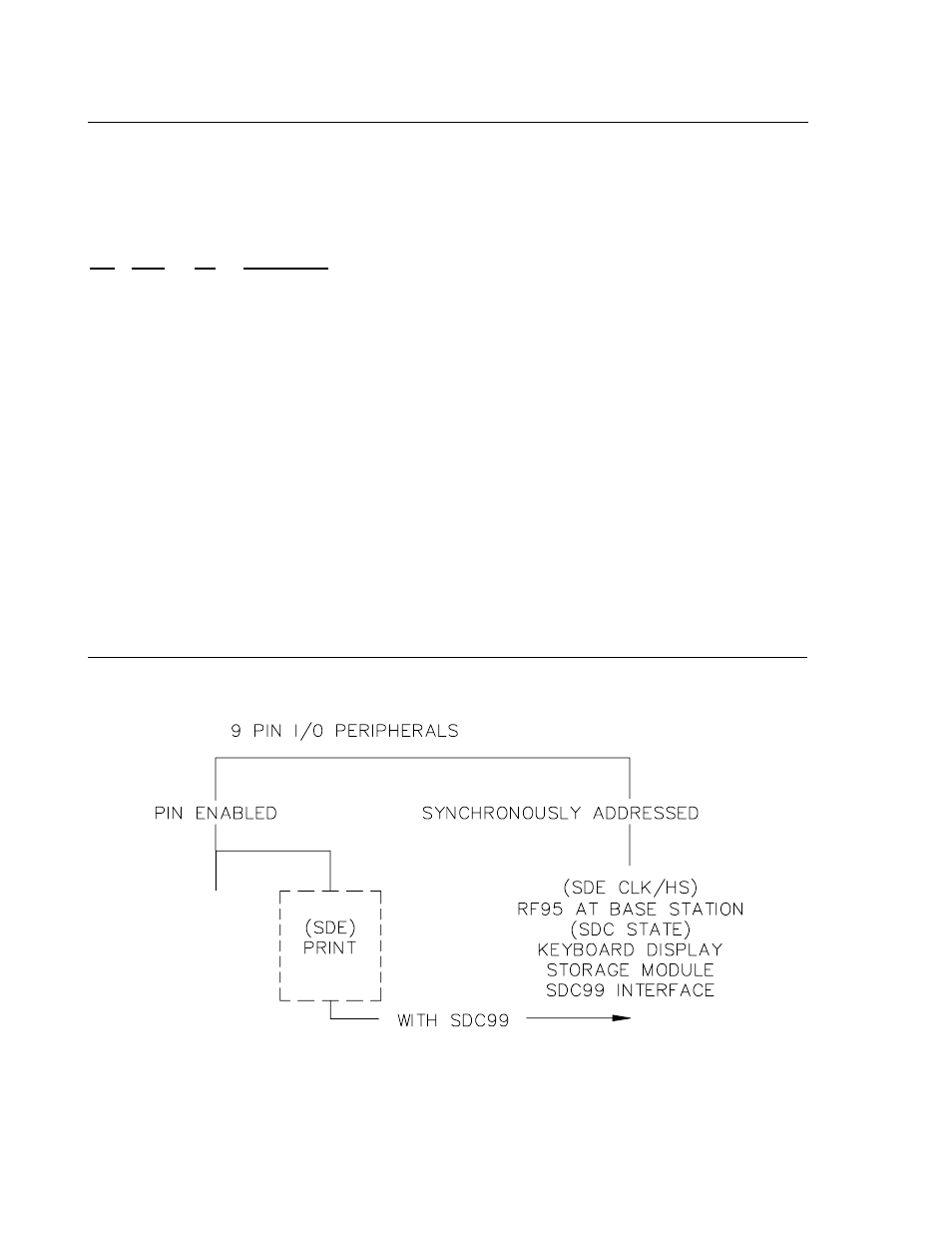
Synchronous Device Enable: Used to address Synchronous Devices (SDs), and
can be used as an enable line for printers.
7
CLK/HS I/O
Clock/Handshake: Used with the SDE and TXD lines to address and transfer
data to SDs. When not used as a clock, pin 7 can be used as a handshake line
(during printer output, high enables, low disables).
8
+12 VDC
9
TXD
O
Transmit Data: Serial data are transmitted from the CR10X to peripherals on pin
9; logic low marking (0V) logic high spacing (5V) standard asynchronous ASCII, 8
data bits, no parity, 1 start bit, 1 stop bit, 300, 1200, 9600, 76,800 baud (user
selectable).
(ME)
MODEM
(COM200
RF95
SC32A)
FIGURE 6.2-1. Hardware Enabled and Synchronously Addressed Peripherals