Rainbow Electronics DS2154 User Manual
Page 4

DS2154
031197 4/69
FUNCTIONAL DESCRIPTION
The analog AMI/HDB3 waveform off of the E1 line is
transformer coupled into the RRING and RTIP pins of
the DS2154. The device recovers clock and data from
the analog signal and passes it through the jitter attenu-
ation mux to the receive side framer where the digital
serial stream is analyzed to locate the framing/multi-
frame pattern. The DS2154 contains an active filter that
reconstructs the analog received signal for the non–lin-
ear losses that occur in transmission. The device has a
usable receive sensitivity of 0 dB to –43 dB which allows
the device to operate on cables over 2km in length. The
receive side framer locates the FAS frame and CRC and
CAS multiframe boundaries as well as detects incoming
alarms including, carrier loss, loss of synchronization,
AIS, and Remote Alarm. If needed, the receive side
elastic store can be enabled in order to absorb the
phase and frequency differences between the recov-
ered E1 data stream and an asynchronous backplane
clock which is provided at the RSYSCLK input. The
clock applied at the RSYSCLK input can be either a
2.048 MHz clock or a 1.544 MHz clock. The RSYSCLK
can also be a bursty clock with speeds up to 8.192 MHz.
The transmit side of the DS2154 is totally independent
from the receive side in both the clock requirements and
characteristics. Data off of a backplane can be passed
through a transmit side elastic store if necessary. The
transmit formatter will provide the necessary frame/mul-
tiframe data overhead for E1 transmission. Once the
data stream has been prepared for transmission, it is
sent via the jitter attenuation mux to the waveshaping
and line driver functions. The DS2154 will drive the E1
line from the TTIP and TRING pins via a coupling trans-
former. The line driver can handle both 75
Ω
and
120
Ω
lines and it has options for high return loss
applications. The line driver contains a current limiter
that will restrict the maximum current into a 1
Ω
load to
less than 50 mA (rms).
READER’S NOTE
This data sheet assumes a particular nomenclature of
the E1 operating environment. There are 32 eight–bit
timeslots in an E1 systems which are number 0 to 31.
Timeslot 0 is transmitted first and received first. These
32 timeslots are also referred to as channels with a num-
bering scheme of 1 to 32. Timeslot 0 is identical to chan-
nel 1, timeslot 1 is identical to Channel 2, and so on.
Each timeslot (or channel) is made up of eight bits which
are numbered 1 to 8. Bit number 1 is the MSB and is
transmitted first. Bit number 8 is the LSB and is trans-
mitted last. Throughout this data sheet, the following
abbreviations will be used:
FAS
Frame Alignment Sig-
nal
CRC4
Cyclical Redundancy
Check
CAS
Channel Associated
Signaling
CCS
Common Channel
Signaling
MF
Multiframe
Sa
Additional bits
Si
International bits
E–bit
CRC4 Error bits
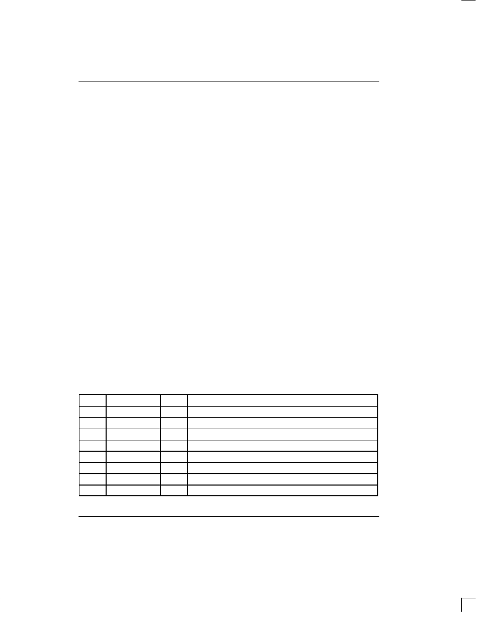
PIN LIST Table 1–1
PIN
SYMBOL
TYPE
DESCRIPTION
1
RCHBLK
O
Receive Channel Block.
2
NC
–
No Connect.
3
8MCLK
O
8.192 MHz Clock.
4
NC
–
No Connect.
5
NC
–
No Connect.
6
RCL
O
Receive Carrier Loss.
7
NC
–
No Connect.
8
NC
–
No Connect.
