Rainbow Electronics DS2154 User Manual
Page 16
DS2154
031197 16/69
ADDRESS
REGISTER ABBREVIATION
REGISTER NAME
R/W
9E
R/W
Receive Channel 31.
RC31
9F
R/W
Receive Channel 32.
RC32
A0
R/W
Transmit Channel Control 1.
TCC1
A1
R/W
Transmit Channel Control 2.
TCC2
A2
R/W
Transmit Channel Control 3.
TCC3
A3
R/W
Transmit Channel Control 4.
TCC4
A4
R/W
Receive Channel Control 1.
RCC1
A5
R/W
Receive Channel Control 2.
RCC2
A6
R/W
Receive Channel Control 3.
RCC3
A7
R/W
Receive Channel Control 4.
RCC4
A8
R/W
Common Control 4.
CCR4
A9
R
Transmit DS0 Monitor.
TDS0M
AA
R/W
Common Control 5.
CCR5
AB
R
Receive DS0 Monitor.
RDS0M
AC
R/W
Test 3.
TEST3 (set to 00h)
AD
R/W
Not Used.
(set to 00h)
AE
R/W
Not Used.
(set to 00h)
AF
R/W
Not Used.
(set to 00h)
NOTES:
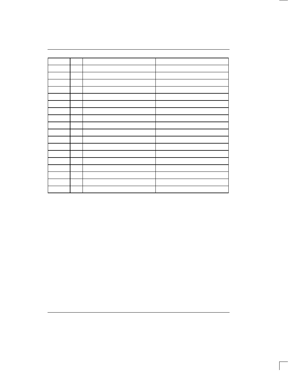
1. Test Registers 1, 2, and 3 are used only by the factory; these registers must be cleared (set to all zeros) on pow-
er–up initialization to insure proper operation.
2. Register banks Bxh, Cxh, Dxh, Exh, and Fxh are not accessible.
2.0
PARALLEL PORT
The DS2154 is controlled via either a non–multiplexed
(MUX=0) or a multiplexed (MUX=1) bus by an external
microcontroller or microprocessor. The DS2154 can
operate with either Intel or Motorola bus timing configu-
rations. If the BTS pin is tied low, Intel timing will be
selected; if tied high, Motorola timing will be selected.
All Motorola bus signals are listed in parenthesis (). See
the timing diagrams in the A.C. Electrical Characteris-
tics in Section 14 for more details.
3.0
CONTROL, ID AND TEST REGISTERS
The operation of the DS2154 is configured via a set of
nine control registers. Typically, the control registers
are only accessed when the system is first powered up.
Once the DS2154 has been initialized, the control regis-
ters will only need to be accessed when there is a
change in the system configuration. There are two
Receive Control Register (RCR1 and RCR2), two
Transmit Control Registers (TCR1 and TCR2), and five
Common Control Registers (CCR1 to CCR5). Each of
the nine registers are described in this section.
There is a device IDentification Register (IDR) at
address 0FH. The MSB of this read–only register is
fixed to a one indicating that the DS2154 is present. The
pin–for–pin compatible T1 version of the DS2154 also
has an ID register at address 0FH and the user can read
the MSB to determine which chip is present since in the
DS2154 the MSB will be set to a one and in the DS2152
it will be set to a zero. The lower four bits of the IDR are
used to display the die revision of the chip.
The Test Registers at addresses 15, 19, and AC hex are
used by the factory in testing the DS2154. On power–
up, the Test Registers should be set to 00 hex in order for
the DS2154 to operate properly.