Write access followed by burst read access – Rainbow Electronics AT75C310 User Manual
Page 27
AT75C310
27
Dynamic Memory Accesses
Figure 5 and Figure 6 describe the different bus operations
that can be performed by DMC.
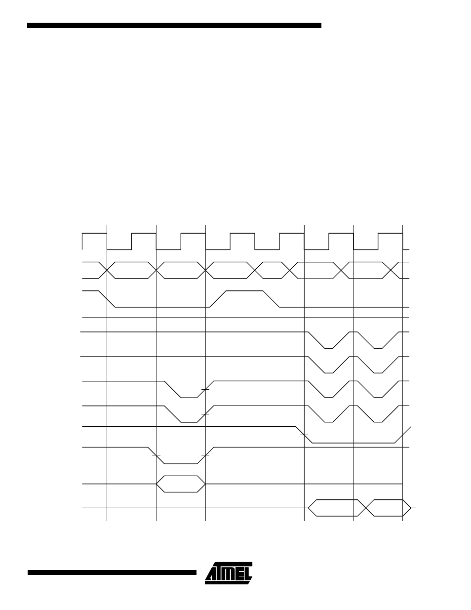
Write Access Followed by Burst Read Access
Figure 5 shows a write to DRAM0 followed by a burst of
two reads from the same device.
The write access takes two clock cycles. During the first
cycle, the row address is output and the RAS strobe is
asserted. In the next cycle, the column address is output
and the CAS strobes are asserted. The read is a half-word
(16-bit) access to an odd half-word address so only CAS2
and CAS3 are active.
The read access is not sequential to the write access
(regardless of the addresses) and the RAS strobe is there-
fore raised for a precharge cycle between the accesses.
The read accesses take two clock cycles to read the first
word of data and one additional clock cycle for the second
word. The row address and RAS are asserted in the same
manner as for the read access. The column address and
CAS strobes are asserted earlier for a read access than for
a write access in order to provide time for the data to read
the processor core. The read accesses shown are word
(32-bit) accesses and all four CAS strobes are therefore
active.
The DMC asserts BWAIT to the ARM during the row
address and precharge cycles.
Figure 5. Write to DRAM0 Waveform
BCLK
RAS0
RAS1
CAS1
CAS2
CAS3
NDOE
NDWE
D (SIAP)
D (MEM)
A
CAS0