Clock generation, Peripheral data controller, E 21 – Rainbow Electronics AT75C310 User Manual
Page 107: Spi programmer’s model
AT75C310
107
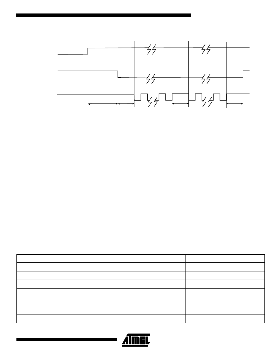
Figure 27. Programmable Delays (DLYBCS, DLYBS and DLYBCT)
Clock Generation
In master mode, the SPI master clock is either ACLK or
ACLK/32 as defined by the MCK32 field of SP_MR. The
SPI baud rate clock is generated by dividing the SPI master
clock by a value between 4 and 510. The divisor is defined
in the SCBR field in each chip select register. The transfer
speed can thus be defined independently for each chip
select signal.
CPOL and NCPHA in the chip select registers define the
clock/data relationship between master and slave devices.
CPOL defines the inactive value of the SPCK. NCPHA
defines the edge that causes data to change and the edge
that causes data to be captured.
In slave mode, the input clock low and high pulse duration
must be longer than two system clock (ACLK) periods.
Peripheral Data Controller
The SPI is connected to two PDC channels. One is dedi-
cated to the receiver, the other is dedicated to the transmit-
ter.
The PDC channel is programmed using SP_TPR (Transmit
Pointer) and SP_TCR (Transmit Counter) for the transmit-
ter and SP_RPR (Receive Pointer) and SP_RCR (Receive
Counter) for the receiver. The status of the PDC is given in
SP_SR by the SPENDTX bit for the transmitter and by the
SPENDRX bit for the receiver.
The pointer registers (SP_TPR and SP_RPR) are used to
store the address of the transmit or receive buffers. The
counter registers (SP_TCR and SP_RCR) are used to
store the size of these buffers.
The receiver data transfer is triggered by the RDRF bit and
the transmitter data transfer is triggered by TDRE. When a
transfer is performed, the counter is decremented and the
pointer is incremented. When the counter reaches 0, the
status bit is set (SPENDRX for the receiver, SPENDTX for
the transmitter in SP_SR) and can be programmed to gen-
erate an interrupt. While the counter is at zero, the status
bit is asserted and transfers are disabled.
SPI Programmer’s Model
SPI Base Address: 0xFF020000
Chip Select 1
Chip Select 2
SPCK Output
DLYBCS
DLYBS
DLYBCT
Change peripheral
No change
of peripheral
DLYBCT
Table 21. SPI Memory Map
Offset
Register Description
Register Name
Access
Reset State
0x00
Control Register
SP_CR
Write-only
–
0x04
Mode Register
SP_MR
Read/write
0
0x08
Receive Data Register
SP_RDR
Read-only
0
0x0C
Transmit Data Register
SP_TDR
Write-only
–
0x10
Status Register
SP_SR
Read-only
0
0x14
Interrupt Enable Register
SP_IER
Write-only
–
0x18
Interrupt Disable Register
SP_IDR
Write-only
–