Switching waveforms – Rainbow Electronics AT75C310 User Manual
Page 22
AT75C310
22
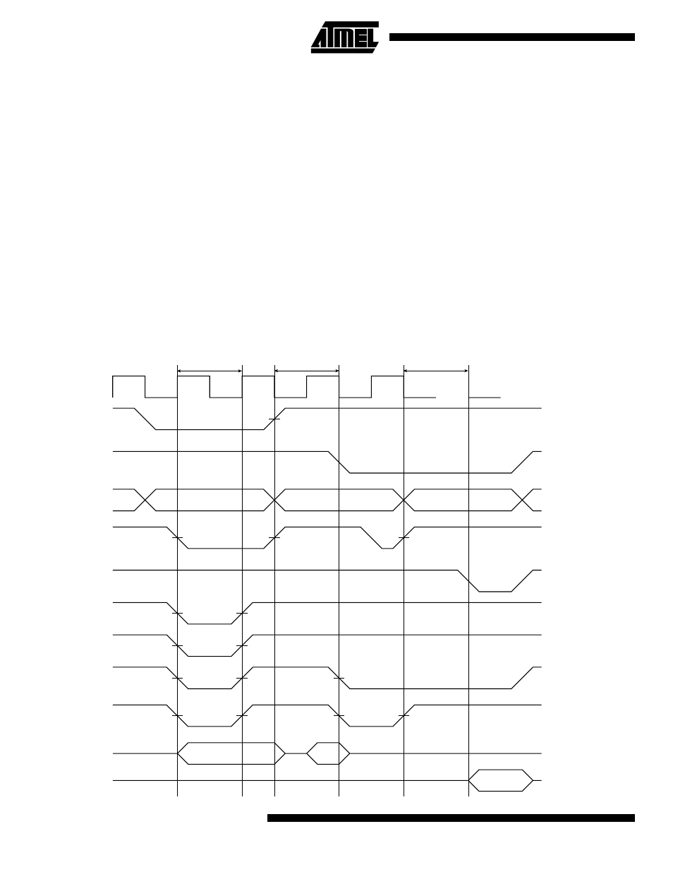
Switching Waveforms
Figure 3 shows a write to memory 0, followed by a write
and a read to memory 1. SMC_CSR0 is programmed for
one wait state with BAT = 0 and DFT = 0. SMC_CSR1 is
programmed for zero wait states with BAT = 1 and
DFT = 0. SMC_MCR is programmed for early reads from
all memories.
The write to memory 0 is a 32-bit word access and, there-
fore, all four NWE strobes are active. As BAT = 0, they are
configured as write strobes and have the same timing as
NWR. As the access employs a single wait state, the write
strobe pulse is one clock cycle long.
There is a chip select change wait state between the mem-
ory 0 write and the memory 1 write. The new address is
output at the end of the memory 0 access but the strobes
are delayed for one clock cycle.
The write to memory 1 is a half-word (16-bit) access to an
odd half-word address and, therefore, NWE2 and NWE3
are active. As BAT = 1 they are configured as byte-select
signals and have the same timing as NCE. As the access
has no internal wait states, the write strobe pulse is one-
half clock cycle long. Data and address are driven until the
write strobe rising edge is sensed at the SIAP pin to guar-
antee positive hold times.
There is an early read wait state between the memory 1
write and the memory 1 read to provide time for the
AT75C310 to disable the output data before the memory is
read. If the read was normal mode, i.e., not early, the
NSOE strobe would not fall until the rising edge of BCLK
and no wait state would be inserted. If the write and early
read were to different memories, then the early read wait
state is not required as a chip select wait state will be
implemented.
The read from memory 1 is a byte access to an address
with a byte offset of two and, therefore, only NWE2 is
active.
Figure 3. Write to Memory 0, Write and Read to Memory 1
BCLK
NCE0
NCE1
A
NWR
NSOE
NWE0
NWE1
NWE2
NWE3
D (SIAP)
D (MEM)