Rainbow Electronics AT75C310 User Manual
Page 23
AT75C310
23
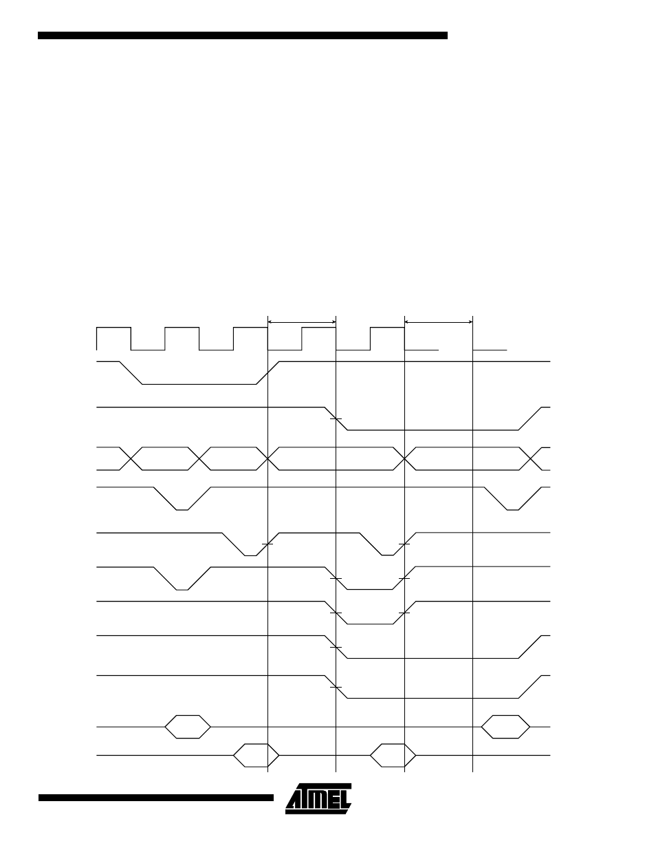
Figure 4 shows a write and a read to memory 0, followed
by a read and a write to memory 1. SMC_CSR0 is pro-
grammed for zero wait states with BAT = 0 and DFT = 0.
SMC_CSR1 is programmed for zero wait states with
BAT = 1 and DFT = 1. SMC_MCR is programmed for nor-
mal reads from all memories
The write to memory 0 is a byte access and, therefore, only
one NWE strobe is active. As BAT = 0, they are configured
as write strobes and have the same timing as NWR.
The memory 0 read immediately follows the write as early
reads are not configured and an early read wait state is not
required. As early reads are not configured, the read strobe
pulse is one-half clock cycle long.
There is a chip select change wait state between the mem-
ory 0 write and the memory 1 read. The new address is
output at the end of the memory 0 access but the strobes
are delayed for one clock cycle.
The write to memory 1 is a half-word (16-bit) access to an
even half-word address and, therefore, NWE0 and NWE1
are active. As BAT = 1, they are configured as byte select
signals and have the same timing as NCE.
As DFT = 1 for memory 1, a wait state is implemented
between the read and write to provide time for the memory
to stop driving the data bus. DFT wait states are only imple-
mented at the end of read accesses.
The read from memory 1 is a byte access to an address
with a byte offset of two and, therefore, only NWE2 is
active.
Figure 4. Write and Read to Memory 0, Read and Write to Memory 1
BCLK
NCE0
NCE1
A
NWR
NSOE
NWE0
NWE1
NWE2
NWE3
D (SIAP)
D (MEM)
Chip Select
Wait State
Data Float
Wait State