Qdrii read operation – Xilinx Virtex-5 FPGA ML561 User Manual
Page 86
86
Virtex-5 FPGA ML561 User Guide
UG199 (v1.2.1) June 15, 2009
Chapter 7: ML561 Hardware-Simulation Correlation
R
QDRII Read Operation
This subsection shows the test results for the QDR2_Q_BY0_B5 signal from QDRII
memory (U35) to FPGA3 (U34) measured at 300 MHz (600 Mb/s), where the unit interval
(UI) = 1.67 ns.
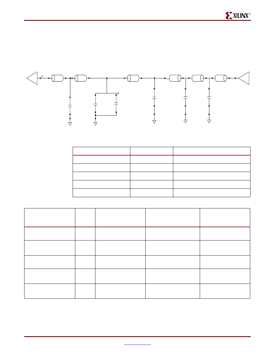
Figure 7-48:
Post-Layout IBIS Schematics of QDRII Read Data Bit (QDR2_Q_BY0_B5)
Virtex-5 FPGA
QDR2_Q_BY0_B5
U34.G33
28.5 ohms
4.473 ps
0.028 in
QDR2_Q_BY0_B5
49.1 ohms
95.834 ps
0.613 in
QDR2_Q_BY0_B5
28.5 ohms
4.404 ps
0.027 in
QDR2_Q_BY0_B5
49.1 ohms
427.654 ps
2.737 in
QDR2_Q_BY0_B5
71.6 ohms
22.319 ps
AutoPadstk_3
71.8 ohms
22.319 ps
AutoPad...
TL1
TL2
TL3
TL6
TL7
TL8
22.9 fF
96.3 fF
500.0 fF
513.2 fF
C7
QDR2_Q...
QDR2_Q...
QDR2_Q...
96.3 fF
QDR2_Q...
22.9 fF
QDR2_Q...
U35.F11
UG199_c7_48_071907
K7R323684M_1.8V
C5
Table 7-13:
Circuit Elements of QDRII Read Data Bit (QDR2_Q_BY0_B5)
Element
Designation
Description
Driver
U36.F11
QDRII memory
Receiver U34.G33
FPGA
HSTL_I_DCI_18
Probe Point
C7
Via under FPGA3 (U34)
PCB Termination
None
DCI at FPGA
Trace Length
TL 1, 3, 6, 8
3.41 inches
Table 7-14:
QDRII Read Operation Correlation Results
Measurement
DVW
(% UI)
ISI
(% UI)
Noise Margin
(VIH + VIL) = Total
(% of VREF)
Overshoot / Undershoot
Margin
(% of VREF)
Hardware at probe point
1.09 ns
(65.4%)
(70 + 50) = 120 ps (7.2%)
(400 + 400) = 800 mV
(88.9%)
(500 + 500) = 1000 mV
(111.1%)
Simulation correlation
slow-weak corner
984 ps
(59.0%)
(72 + 75) = 147 ps (8.8%)
(250 + 264) = 514 mV
(57.1%)
(532 + 518) = 1050 mV
(105.5%)
Correlation Delta:
HW vs. Simulation
106 ps
(6.4%)
27 ps (1.6%)
386 mV (31.8%)
50 mV (5.6%)
Extrapolation at IOB
slow-weak corner
1.46 ns
(88%)
(49 + 36) = 85 ps (5.1%)
(237 + 272) = 509 mV
(56.5%)
(608 + 575) = 1183 mV
(131.5%)
Extrapolation at IOB
fast-strong corner
1.45 ns
(87%)
(27 + 39) = 66 ps (4.0%)
(341 +201) = 542 mV
(60.3%)
(532 + 661) = 1193 mV
(132.6%)