Controller – operation – Xilinx Virtex-5 FPGA ML561 User Manual
Page 123
Virtex-5 FPGA ML561 User Guide
123
UG199 (v1.2.1) June 15, 2009
Hardware Schematic Diagram
R
Controller – Operation
The pixels for the LCD panel are stored in the controller data RAM. This RAM is a 65-row
by 132-column array. Each display pixel is represented by a single bit in the RAM array.
The interface to the RAM array goes through the 8-bit (DB0 – DB7) LCD interface.
Therefore, the 65-bit rows are split into eight pages of eight lines. The ninth page is a single
line page (DB0 only).
Interface designs can read from or write to the RAM array.
The display page is changed through the 4-bit page address register.
The column address (line address) is set with a two-byte register access. The line address
corresponds to the first line that is going to be displayed on the LCD panel. This address is
located in a 6-bit address register.
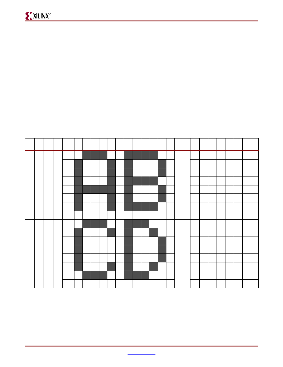
The RAM array is configured such that there are two characters per row (page), where each
character pair uses eight rows of the display panel.
address lines, ADC control, and LCD outputs (segments).
Table C-2:
LCD Panel
DB3 DB2 DB1 DB0 Data
Line
Address
0
0
0
0
DB0
Page 0
00H
DB1
01H
DB2
02H
DB3
03H
DB4
04H
DB5
05H
DB6
06H
DB7
07H
0
0
0
1
DB0
Page 1
08H
DB1
09H
DB2
0AH
DB3
0BH
DB4
0CH
DB5
0DH
DB6
0EH
DB7
0FH