Instruction set – Xilinx Virtex-5 FPGA ML561 User Manual
Page 130
130
Virtex-5 FPGA ML561 User Guide
UG199 (v1.2.1) June 15, 2009
Appendix C: LCD Interface
R
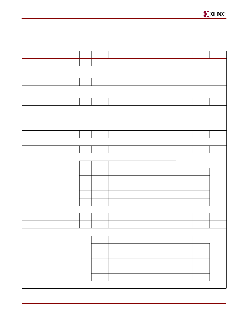
Instruction Set
shows the instruction set for the LCD panel.
Table C-6:
Display Instructions
Instruction
RS
RW
DB7
DB6
DB5
DB4
DB3
DB2
DB1
DB0
Read display data
1
1
Read Data
8-bit data specified by the column and page address can be read from the Display Data RAM. The column address is increased automatically,
thus data can be read continuously from the addressed page.
Write display data
1
0
Write Data
8-bit data can be written into a RAM location specified by the column and page address. The column address is increased automatically, thus
data can be written continuously to the addressed page.
Read status
0
1
BUSY
ADC
ONOFF
RESETB
0
0
0
0
BUSY: Device is BUSY when internal operation or reset. (0=active, 1 =busy).
ADC: Indicates the relationship between RAM column address and segment driver.
ONOFF: Indicates display ON or OFF status.
RESETB: Indicates if initialization is in progress.
Display ON/OFF
0
0
1
0
1
0
1
1
1
DON
Turn display ON or OFF. (1=ON, 0 = OFF)
Initial display line
0
0
0
1
ST5
ST4
ST3
ST2
ST1
ST0
Sets the line address of the display RAM to determine the initial line of the LCD panel.
ST5
ST4
ST3
ST2
ST1
ST0
0
0
0
0
0
0
Line address 0
0
0
0
0
0
1
Line address 1
..
..
..
..
..
..
..
1
1
1
1
1
0
Line address 62
1
1
1
1
1
1
Line address 63
Set reference voltage mode
0
0
1
0
0
0
0
0
0
1
Set reference voltage register
0
0
x
x
SV5
SV4
SV3
SV2
SV1
SV0
This is a two-byte instruction. The first instruction sets the reference voltage mode. The second instruction sets the reference voltage parameter.
SV5
SV4
SV3
SV2
SV1
SV0
0
0
0
0
0
0
0
0
0
0
0
0
1
1
..
..
..
..
..
..
..
1
1
1
1
1
0
62
1
1
1
1
1
1
63