Xilinx Virtex-5 FPGA ML561 User Manual
Page 35
Virtex-5 FPGA ML561 User Guide
35
UG199 (v1.2.1) June 15, 2009
Power Regulation
R
The FPGA can drive VMARGIN_DN_xxxx_N and VMARGIN_UP_xxxx_N signals, where
xxxx indicates one of the six main power regulators: SSTL2, HSTL, SSTL18, VCC1V0,
VCC2V5, and VCC3V3.
If both voltage-margining inputs to the power regulator are pulled Low, the output voltage
is close to nominal but has the possibility of a slightly higher error in the output voltage.
The power modules use a low-leakage open-drain control signal to control the voltage
margining. In the FPGA, this can be approximated by using a control signal that drives the
output Low when active and does not drive the signal at all when inactive (high-
impedance output).
Three-pin headers are available for performing manual voltage margining, using jumpers
to select between Nominal, -5%, and +5%.
shows the jumper settings.
The TI PTH05010-WAZ and TI PTH05000-ADJ regulator outputs can be enabled or
inhibited through the use of on-board two-pin jumpers. The inhibit jumpers use the
following conventions:
•
Jumper OFF = Enabled
•
Jumper ON = Inhibited
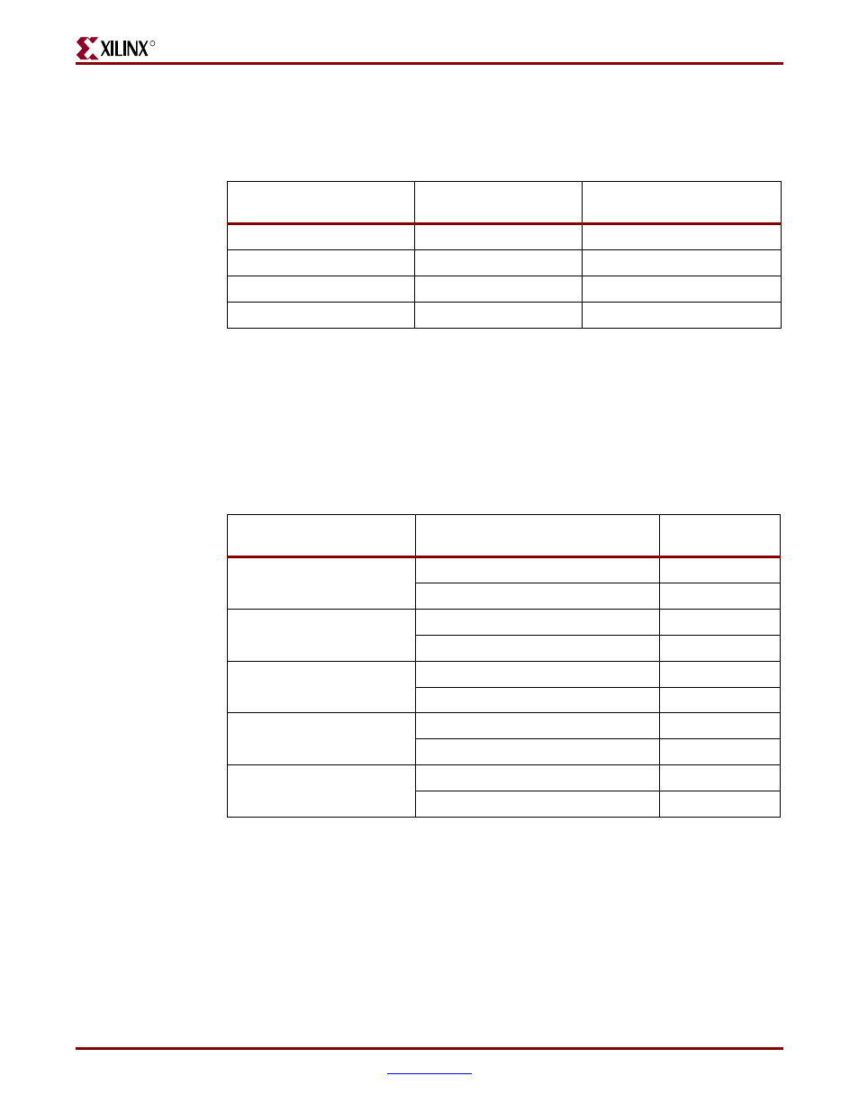
Table 3-16:
Manual Voltage Margining
VMARGIN_UP_N
VMARGIN_DN_N
Output Voltage
High
High
Nominal
High
Low
-5%
Low
High
+5%
Low
Low
Not Applicable
Table 3-17:
FPGA #1 Signals and On-Board Jumpers for Voltage Margining
Power Regulator
Signal Name
Jumper Setting
V
CCINT
(VR6)
VMARGIN_UP_VCC1V0_N
P48: 1 -> 2
VMARGIN_DN_VCC1V0_N
P48: 3 -> 2
SSTL18 (VR1)
VMARGIN_UP_SSTL18_N
P4: 1 -> 2
VMARGIN_DN_SSTL18_N
P4: 3 -> 2
SSTL2 (VR9)
VMARGIN_UP_SSTL2_N
P450 1 -> 2
VMARGIN_DN_SSTL2_N
P50: 3 -> 2
HSTL (VR10)
VMARGIN_UP_HSTL_N
P58: 1 -> 2
VMARGIN_DN_HSTL_N
P58: 3 -> 2
V
CCAUX
(VR12)
VMARGIN_UP_VCC2V5_N
P69: 1 -> 2
VMARGIN_DN_VCC2V5_N
P69: 3 -> 2