Controller – lcd panel connections – Xilinx Virtex-5 FPGA ML561 User Manual
Page 125
Virtex-5 FPGA ML561 User Guide
125
UG199 (v1.2.1) June 15, 2009
Hardware Schematic Diagram
R
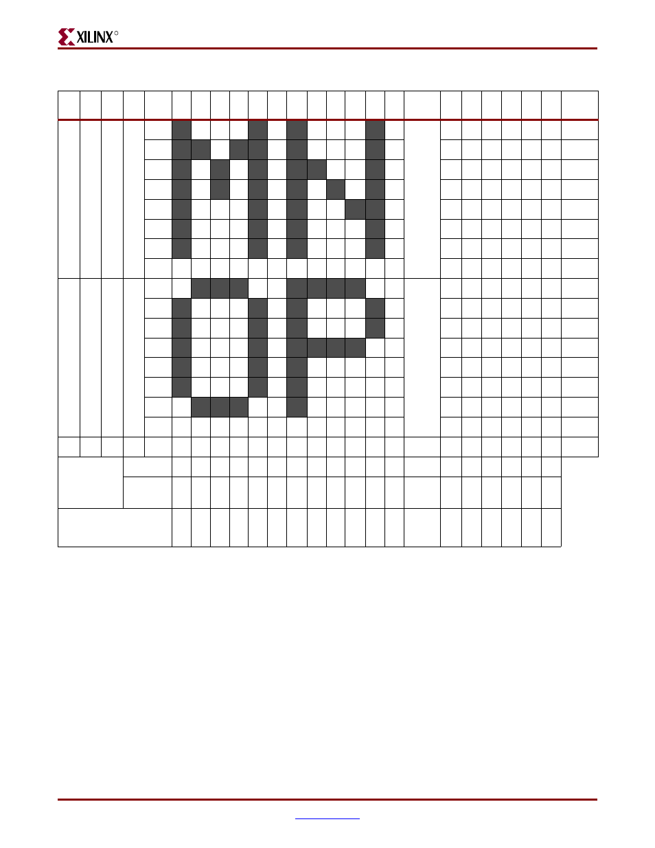
When a page is addressed, all the bits representing dots on the LCD panel can be accessed
in that page. An array of 8x132 bits is available. The line address dictates what line of the
RAM is going to be displayed on the first line of the glass panel.
Controller – LCD Panel Connections
The controller die, KS0713, connects to the LCD glass panel and user connection pins via a
small PCB. Other necessary pins have default connections on the PCB.
0
1
1
0
DB0
Page 6
30H
DB1
31H
DB2
32H
DB3
33H
DB4
34H
DB5
35H
DB6
36H
DB7
37H
0
1
1
1
DB0
Page 7
38H
DB1
39H
DB2
3AH
DB3
3BH
DB4
3CH
DB5
3DH
DB6
3EH
DB7
3FH
1
0
0
0
DB0
Page 8
Column
Address
ADC = 0
0
1
2
3
4
5
6
7
8
9
A
B
7E
7F
80
81
82
83
ADC = 1
83
82
81
80
7F
7
E
7
D
7
C
7
B
7
A
79
78
5
4
3
2
1
0
LCD Output
Seg 1
Seg 2
Seg 3
Seg 4
Seg 5
Seg 6
Seg 7
Seg 8
Seg 9
Seg 10
Seg 1
1
Seg 12
Seg 12
7
Seg 12
8
Seg 12
9
Seg 13
0
Seg 13
1
Seg 13
2
Table C-2:
LCD Panel (Continued)
DB3 DB2 DB1 DB0 Data
Line
Address