Xilinx Virtex-5 FPGA ML561 User Manual
Page 128
128
Virtex-5 FPGA ML561 User Guide
UG199 (v1.2.1) June 15, 2009
Appendix C: LCD Interface
R
•
The voltage follower and voltage regulator are set to:
♦
Five times boost mode
♦
The V4, V3, V2, V1, and V0 outputs depend on the bias settings of 1/9 or 1/7.
Because of these default settings, the following display controller connections are not used:
•
DISP: Turns into an output when Master mode is selected
•
FRS: Static driver segment output
•
M: Used in Master/Slave display configurations
•
CL: Clock pin used in Master/Slave display configurations
When RESETB is Low, the display controller is initialized as indicated in
.
When RESETB is High, the display must be initialized. The first steps to be taken to
guarantee correct operation of the display and the controller are:
•
Configure the ADC bit. This bit determines the scanning direction of the segments.
♦
When the RESETB signal is active, ADC is reset to 0, meaning that the segments
are scanned from SEG1 up to SEG132.
♦
When ADC is set to 1, the segments are scanned in opposite direction.
•
Configure the SHL bit. This bit sets the scanning direction of the COM lines.
♦
When the RESETB signal is active, SHL is reset to 0, meaning that the segments
are scanned from COM1 up to COM64.
♦
When SHL is set to 1, the common lines are scanned in opposite direction.
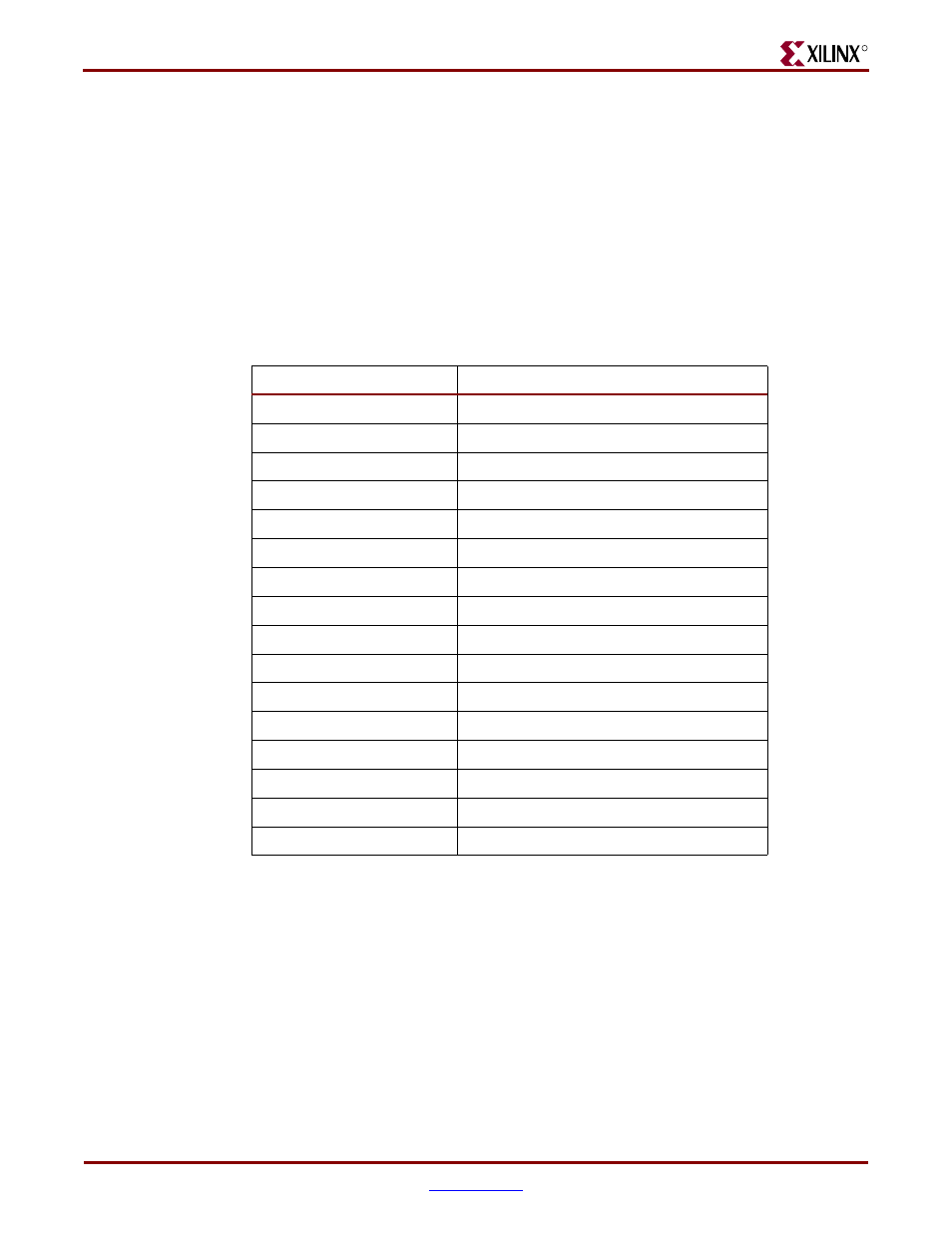
Table C-3:
Display Controller Initialization (RESETB is Low)
Parameter
Initial Value
Display
OFF
Entire Display
OFF
ADC Select
OFF
Reverse Display
OFF
Power Control
0,0,0 (VC, VR, VF)
LCD Bias
1/7
Read-Modify-Write
OFF
SHL Select
OFF
Static Indicator Mode
OFF
Static Indicator Register
0,0 (S1, S0)
Display Start
0 (First line)
Column Address
0
Page Address
0
Regulator Select
0,0,0 (R2, R1, R0)
Reference Voltage
OFF
Reference Voltage Register
1,0,0,0,0,0 (SV5, SV4, SV3, SV2, SV1, SV0)