Table 5-5, Table 5-4 – Xilinx Virtex-5 FPGA ML561 User Manual
Page 49
Virtex-5 FPGA ML561 User Guide
49
UG199 (v1.2.1) June 15, 2009
Termination and Transmission Line Summaries
R
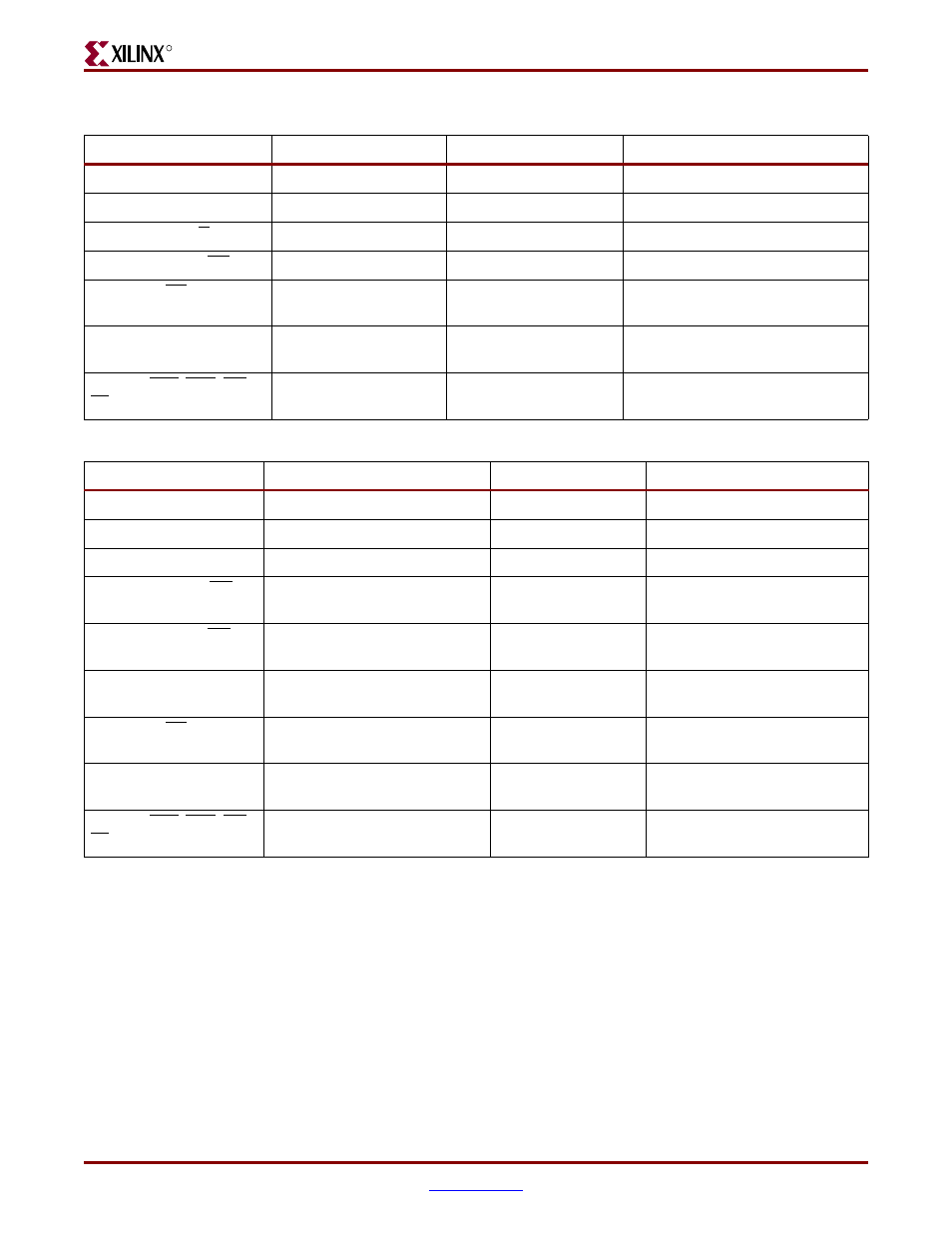
Table 5-4:
QDRII SRAM Terminations
Signal
FPGA Driver
Termination at FPGA
Termination at Memory
Write Data (D)
HSTL_I_18
No termination
50
Ω pull-up to 0.9V
Read Data (Q)
HSTL_I_DCI_18
No termination
No termination
Write Strobe (K, K)
HSTL_I_18
No termination
50
Ω pull-up to 0.9V
Read Strobe (CQ, CQ)
HSTL_I_DCI_18
No termination
No termination
Clock (CK, CK)
HSTL_I_18
No termination
100
Ω differential termination
between pair
Address (A, BA)
HSTL_I_18
No termination
50
Ω pull-up to 0.9V after the last
component
Control (RAS, CAS, WE,
CS, CKE, and BW)
HSTL_I_18
No termination
50
Ω pull-up to 0.9V after the last
component
Table 5-5:
RLDRAM II Terminations
Signal FPGA
Driver
Termination
at FPGA
Termination at Memory
Data (DQ for CIO)
HSTL_II_DCI_18
No termination
50
Ω pull-up to 0.9V
Data (Q for SIO)
HSTL_I_DCI_18
No termination
No termination
Write Data (D for SIO)
HSTL_I_18
No termination
50
Ω pull-up to 0.9V
Write Strobe (DK, DK)
DIFF_HSTL_I_18
No termination
100
Ω differential termination
between pair
Read Strobe (QK, QK)
DIFF_HSTL_II_DCI_18 (for CIO)
DIFF_HSTL_I_DCI_18 (for SIO)
No termination
No termination
Data Valid (QVLD)
HSTL_II_DCI_18 (for CIO)
HSTL_I_DCI_18 (for SIO)
No termination
No termination
Clock (CK, CK)
DIFF_HSTL_I_18
No termination
100
Ω differential termination
between pair
Address (A, BA)
HSTL_I_18
No termination
50
Ω pull-up to 0.9V after the last
component
Control (RAS, CAS, WE,
CS, and CKE)
HSTL_I_18
No termination
50
Ω pull-up to 0.9V after the last
component