Ddr2 dimm write operation, Chapter 7: ml561 hardware-simulation correlation – Xilinx Virtex-5 FPGA ML561 User Manual
Page 70
70
Virtex-5 FPGA ML561 User Guide
UG199 (v1.2.1) June 15, 2009
Chapter 7: ML561 Hardware-Simulation Correlation
R
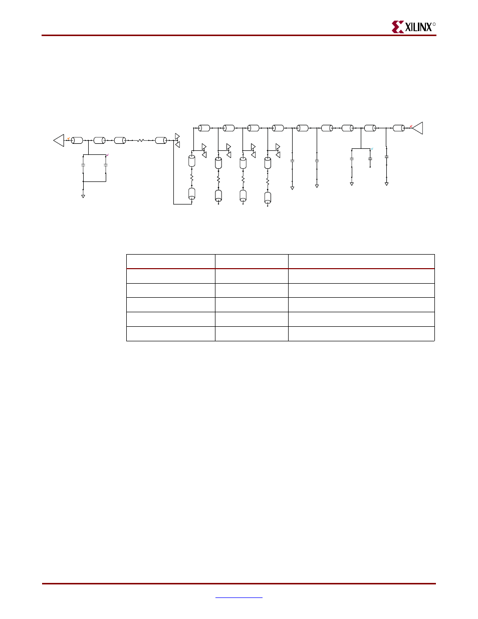
DDR2 DIMM Write Operation
This subsection shows the test results for the DDR2_DIMM_DQ_BY2_B3 signal from
FPGA2 (U5) to the DDR2 DIMM (XP2) measured at 333 MHz (667 Mb/s), where the unit
interval (UI) = 1.5 ns.
The IBIS schematics for DDR2 DIMM interface is extracted from a multi-board project
definition of the two-board combination, which includes the ML561 motherboard and the
DDR2 DIMM at the XP2 connector of the motherboard. The impedance characteristics of
the Molex socket pin (XP2, pin 31) is also included in the IBIS model as a (TL13,
R_00179_CONN_0001, TL14) combination.
The ML561 board under test (S/N 103) is assembled with DDR2 sockets XP3, XP4, and
XP5, which can be utilized for deep DIMM interfaces as described in
and
. To accurately represent the IBIS model of the
DDR2_DIMM_DQ_BY2_B3 signal, the IBIS schematics in
have added stubs for
the three socket pins at the XP3, XP4, and XP5 connectors.
The DDR2 DIMM used for this correlation testing is a single-rank DIMM part (Micron part
number MT9HTF6472xx-667). Thus for hardware measurements closest to the load, a
probe point via on the DIMM for pin U3.J1 is available.
Figure 7-21:
Post-Layout IBIS Schematics of DDR2 DIMM Write Data Bit (DDR2_DIMM_DQ_BY2_B3)
MT47H64M8CB_C...
DQ6
59.8 ohms
3.590 ps
0.022 in
MDQ19_B01
59.8 ohms
31.503 ps
0.195 in
MDQ19_B01
59.8 ohms
78.962 ps
0.490 in
MDQ19_B01
59.8 ohms
10.373 ps
0.064 in
DQ19_B01
49.8 ohms
94.605 ps
0.606 in
DDR2_DIMM_DQ_...
49.8 ohms
90.955 ps
0.582 in
DDR2_DIMM_DQ_...
49.8 ohms
90.340 ps
0.578 in
DDR2_DIMM_DQ_...
49.8 ohms
864.365 ps
5.533 in
DDR2_DIMM_DQ_...
28.5 ohms
4.473 ps
0.028 in
DDR2_DIMM_DQ_...
49.1 ohms
41.316 ps
0.264 in
DDR2_DIMM_DQ_...
49.1 ohms
78.216 ps
0.501 in
DDR2_DIMM_DQ_...
DDR2_DI...
U5_B00.H29
UG199_c7_21_071907
XP5_B00.31
XP4_B00.31
XP3_B00.31
XP2_B00.31
DDR2_DI...
DDR2_DI...
DDR2_DI...
59.1 ohms
12.486 ps
AutoPadstk_12_B...
50.3 ohms
23.650 ps
DQ19_B...
50.3 ohms
23.650 ps
DDR2_D...
50.3 ohms
23.650 ps
DDR2_D...
50.3 ohms
23.650 ps
DDR2_D...
50.3 ohms
23.650 ps
DDR2_D...
50.3 ohms
23.650 ps
DQ19_B...
50.3 ohms
23.650 ps
DQ19_B...
50.3 ohms
23.650 ps
DQ19_B...
71.6 ohms
22.319 ps
AutoPadstk_3_B00
TL1
TL5
TL11
TL12
22.0 ohms
C13
500.0 fF
17.3 fF
MDQ19_...
0.0 milliohms
0.0 milliohms
0.0 milliohms
0.0 milliohms
RN6_B01
R_00179...
R7
R5
R6
TL15
TL16
TL17
TL18
TL24
TL25
TL23
TL27
TL14
????
????
????
????
TL22
TL26
TL13
TL3
TL6
TL7
TL20
TL19
U3_B01.J1
J1_B01.31
????
500.0 fF
C8
96.3 fF
46.4 fF
253.0 fF
22.9 fF
Virtex-5 FPGA
DDR2_DQ_BY2_B3
Table 7-6:
Circuit Elements of DDR2 DIMM Write Data Bit
(DDR2_DIMM_DQ_BY2_B3)
Element
Designation
Description
Driver
U5.H29
FPGA SSTL18_II_DCI_O
Receiver XP2-U3.J1
DDR2 DIMM, 75
Ω ODT
Probe Point
C13
Via under memory on DIMM
PCB Termination
None
ODT at load
Trace Length
Multiple TLs
8.975 inches