Xilinx Virtex-5 FPGA ML561 User Manual
Page 132

132
Virtex-5 FPGA ML561 User Guide
UG199 (v1.2.1) June 15, 2009
Appendix C: LCD Interface
R
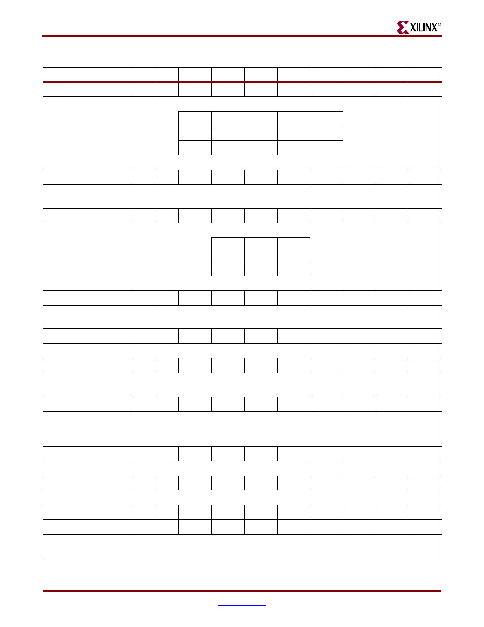
Reverse display ON/OFF
0
0
1
0
1
0
0
1
1
REV
REV
RAM bit data = '1'
RAM bit data = '0'
0
Pixel ON
Pixel OFF
1
Pixel OFF
Pixel ON
Entire display ON/OFF
0
0
1
0
1
0
0
1
0
EON
This instruction forces the display to be turned on regardless the contents of the display data RAM. The contents of the display data RAM are
saved. This instruction has priority over reverse display.
LCD bias select
0
0
1
0
1
0
0
0
1
BIAS
This instruction selects the LCD bias.
Duty
ratio
Bias = 0
Bias = 1
1/65
1/7
1/9
Set modify-read
0
0
1
1
1
0
0
0
0
0
This instruction stops the automatic incrementing of the column address by a read operation. The automatic increment is still done with a
write operation.
Reset modify-read
0
0
1
1
1
0
1
1
1
0
This instruction resets the changed modify-read to the normal.
Reset
0
0
1
1
1
0
0
0
1
0
This instruction resets the LCD controller registers to the default values. The instruction CANNOT initialize the LCD power supply initialized
with RESETB.
SHL select
0
0
1
1
0
0
SHL
x
x
x
This instruction sets the COM output scanning direction.
SHL = 0, COM1 ----> COM64 (default)
SHL = 1, COM64 ----> COM1
Power Control
0
0
0
0
1
0
1
VC
VR
VF
This instruction selects one of the eight power circuit functions. In the case of the DisplayTech 64128EFCBC display, these must be kept at "000"
Regulator resistor select
0
0
0
0
1
0
0
R2
R1
R0
This instruction selects the resistor ratio Rb/Ra.
Set static indicator mode
0
0
1
0
1
0
1
1
0
SM
Set static indicator register
0
0
x
x
x
x
x
x
S1
S0
This is a two-byte instruction. The first instruction enables the second instruction. The second instruction update the contents of the static
indicator register.
Table C-6:
Display Instructions (Continued)
Instruction
RS
RW
DB7
DB6
DB5
DB4
DB3
DB2
DB1
DB0
