Measurement Computing Personal488 rev.3.0 For DOS & Windows 3.Xi User Manual
Page 25
I. HARDWARE GUIDES
2. Personal488 (with GP488B)
Personal488 User’s Manual, Rev. 3.0
I-9
Note:
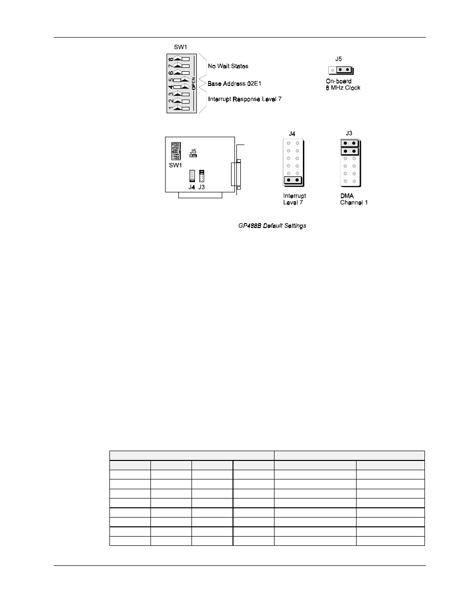
The GP488B, as illustrated, has one DIP switch, two 12-pin headers and one 3-pin header,
labeled SW1, J3, J4, and J5, respectively. The DIP switch setting, along with the arrangement
of the jumpers on the headers, set the hardware configuration.
Default Settings
The figure indicates the GP488B default configuration. Notice that SW1 controls the wait state
generation, the I/O base address and interrupt response level, J4 sets the interrupt request level, J3
selects the DMA channel, and J5 selects the clock source.
I/O Base Address Selection
The I/O base address sets the addresses used by the computer to communicate with the IEEE 488
interface hardware on the board. The address is normally specified in hexadecimal and can be
02E1
,
22E1
,
42E1
, or
62E1
. The registers of the IOT7210 IEEE 488 controller chip and other auxiliary
registers are then located at fixed offsets from the base address.
Most versions of Driver488 are capable of managing as many as four IEEE 488 interface boards. To
do so, the board configurations must be arranged to avoid conflict among themselves. No two boards
may have the same I/O address, but they may, and usually should, have the same DMA channel and
interrupt level.
The factory default I/O base address is
02E1
. To use another, set SW1 switches 4 and 5 according to
the following table and figure.
I/O Base Address
Register
02E1
22E1
42E1
62E1
Read Register
Write Register
02E1
22E1
42E1
62E1
Data In
Data Out
06E1
26E1
46E1
66E1
Interrupt Status 1
Interrupt Mask 1
0AE1
2AE1
4AE1
6AE1
Interrupt Status 2
Interrupt Mask 2
0EE1
2EE1
4EE1
6EE1
Serial Poll Status
Serial Poll Mode
12E1
32E1
52E1
72E1
Address Status
Address Mode
16E1
36E1
56E1
76E1
CMD Pass Through
Auxiliary Mode
1AE1
3AE1
5AE1
7AE1
Address 0
Address 0/1
1EE1
3EE1
5EE1
7EE1
Address 1
End of String