Flash memory, Flash memory –63, Flash memory” on – Altera Stratix III Development Board User Manual
Page 71
Chapter 2: Board Components
2–63
On-Board Memory
May 2013
Altera Corporation
Stratix III 3SL150 Development Board
Reference Manual
lists the SRAM device component reference and manufacturing
information.
Flash Memory
A 512-Mbit Intel P30 flash memory device is used to store configuration files for the
FPGA as well as any other necessary data for the development board operation. The
target device is a PC48F4400P0VB00 in a BGA package and it supports the common
flash interface (CFI) commands. The flash, SSRAM, and the MAX II CPLD all support
1.8-V I/O, and all three devices share a common address and data bus. The default
addressing mode is a 16-bit word mode. Byte mode requires driving BYTEn low.
lists the required flash memory signals.
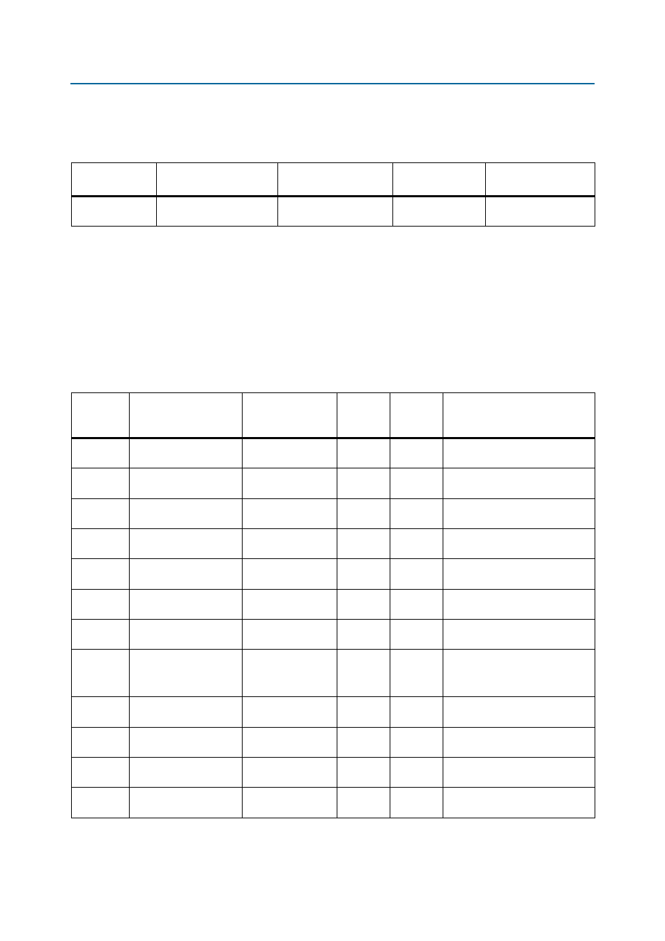
Table 2–54. SRAM Device Component Reference and Manufacturing Information
Board Reference
Description
Manufacturer
Manufacturing
Part Number
Manufacturer
Website
U4, U10
32 MBytes (2M × 16) of
SRAM
Samsung Semiconductor K1B3216B2E-B170
Table 2–55. Flash Interface I/O (Part 1 of 3)
Board
Reference
Description
Schematic Signal
Name
I/O
Standard
Stratix III
Pin
Number
Other Connections
U9 pin B1
Address bus shared with
flash and P-SRAM bit 1
FSM_A1
1.8 V
H23
U5 pin T8 and U4 pin A3 and U10
pin A3 and U5 pin T8
U9 pin C1
Address bus shared with
flash and P-SRAM bit 2
FSM_A2
1.8 V
G23
U5 pin T9 and U4 pin A4 and U10
pin A4 and U5 pin T9
U9 pin D1
Address bus shared with
flash and P-SRAM bit 3
FSM_A3
1.8 V
F23
U5 pin R9 and U4 pin A5 and U10
pin A5 and U5 pin R9
U9 pin D2
Address bus shared with
flash and P-SRAM bit 4
FSM_A4
1.8 V
D27
U5 pin P9 and U4 pin B3 and U10
pin B3 and U5 pin P9
U9 pin A2
Address bus shared with
flash and P-SRAM bit 5
FSM_A5
1.8 V
D28
U5 pin T10 and U4 pin B4 and
U10 pin B4 and U5 pin T10
U9 pin C2
Address bus shared with
flash and P-SRAM bit 6
FSM_A6
1.8 V
F25
U5 pin P13 and U4 pin C3 and
U10 pin C3 and U5 pin P13
U9 pin A3
Address bus shared with
flash and P-SRAM bit 7
FSM_A7
1.8 V
F26
U5 pin R10 and U4 pin C4 and
U10 pin C4 and U5 pin R10
U9 pin B3
Address bus shared with
flash and P-SRAM bit 8
FSM_A8
1.8 V
G24
U5 pin M10 and U4 pin D4 and
U10 pin
D4 and U5 pin M10
U9 pin C3
Address bus shared with
flash and P-SRAM bit 9
FSM_A9
1.8 V
F24
U5 pin M11 and U4 pin H2 and
U10 pin H2 and U5 pin M11
U9 pin D3
Address bus shared with
flash and P-SRAM bit 10
FSM_A10
1.8 V
E26
U5 pin N10 and U4 pin H3 and
U10 pin H3 and U5 pin N10
U9 pin C4
Address bus shared with
flash and P-SRAM bit 11
FSM_A11
1.8 V
D26
U5 pin R11 and U4 pin H4 and
U10 pin H4 and U5 pin R11
U9 pin A5
Address bus shared with
flash and P-SRAM bit 12
FSM_A12
1.8 V
A30
U5 pin P10 and U4 pin H5 and
U10 pin H5 and U5 pin P10