General user interfaces, User-defined push-button switches, General user interfaces –28 – Altera Stratix III Development Board User Manual
Page 36: User-defined push-button switches –28, User-defined push-button
2–28
Chapter 2: Board Components
General User Interfaces
Stratix III 3SL150 Development Board
May 2013
Altera Corporation
Reference Manual
lists the board’s clock distribution system.
f
For more information about the board’s clocking scheme, refer to the Stratix III
development board schematics included with the Stratix III development board kit.
General User Interfaces
To allow you to fully leverage the I/O capabilities of the Stratix III device for
debugging, control, and monitoring purposes, the following general user interfaces
are available on the board:
■
“User-Defined Push-Button Switches” on page 2–28
■
“User-Defined DIP Switches” on page 2–29
■
“User-Defined LEDs” on page 2–30
■
“7-Segment Displays” on page 2–31
■
■
User-Defined Push-Button Switches
The development board includes four general user and one user reset push-button.
For information about the system and reset push-button switches, refer to
Reset and Configuration Switches” on page 2–23
Board references S2 through S5 are push-button switches allowing user interactions
with the Stratix III device. When the switch is pressed and held down, the device pin
is set to a logic 0; when the switch is released, the device pin is set to a logic 1. There is
no board-specific function for these four push-button switches.
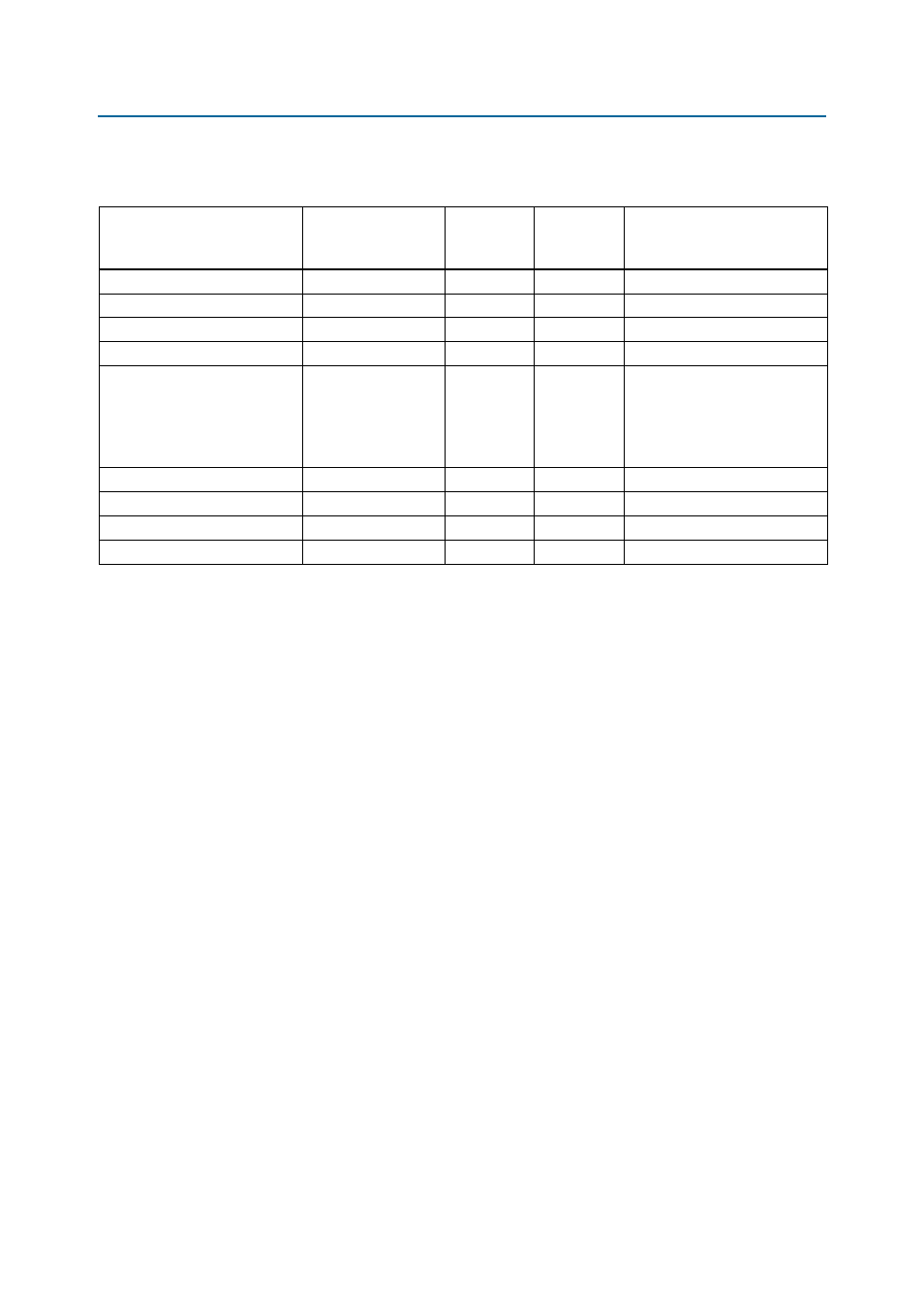
Table 2–20. Stratix III Development Board Clock Distribution
Source
Schematic
Signal Name
I/O Standard
Signal
Originates
From
Signal Propagates To
125-MHz (Y5) oscillator
clkin_125
Input
Y5
Stratix III device pin B16
50-MHz (Y6) oscillator
clkin_50
Input
Y6
Stratix III device pin T33
User input (SMA clock input)
clkin_sma
Input
J16
Stratix III device pin AP15
User output (SMA clock output)
clkout_sma
Output
J17
From Stratix III device pin AE27
25 MHz (reference clock)
This clock can change both
speed and direction depending
on the Ethernet link speed
(10/100/1000)
enet_rx_clk
Input
U25
Stratix III device pin AK28
24-MHz (Y4) oscillator
clkin_24
Input
Y4
MAX II device pin J12 (Bank 3)
6-MHz crystal
XTIN/XTOUT
Input
Y3
FTDI USB PHY
24-MHz crystal
XTALIN/XTALOUT
Input
Y2
Cypress USB PHY
125-MHz (Y1) oscillator
clkin_max_125
Input
Y1
MAX II device pin H12 (Bank 3)