Altera Stratix III Development Board User Manual
Page 18
2–10
Chapter 2: Board Components
MAX II CPLD
Stratix III 3SL150 Development Board
May 2013
Altera Corporation
Reference Manual
T15
Address bus shared with flash
and P-SRAM bit 23
FSM_A23
1.8 V
D31
U9 pin H8
P12
Address bus shared with flash
and P-SRAM bit 24
FSM_A24
1.8 V
F27
U9 pin B6
P4
Data bus shared with flash and
SRAM bit 0
FSM_D0
1.8 V
G27
U9 pin F2 and U4 pin
B6
R1
Data bus shared with flash and
SRAM bit 1
FSM_D1
1.8 V
F28
U9 pin E2 and U4 pin
C5
P5
Data bus shared with flash and
SRAM bit 2
FSM_D2
1.8 V
E28
U9 pin G3 and U4
pin C6
T2
Data bus shared with flash and
SRAM bit 3
FSM_D3
1.8 V
D30
U9 pin E4 and U4 pin
D5
N5
Data bus shared with flash and
SRAM bit 4
FSM_D4
1.8 V
C30
U9 pin E5 and U4 pin
E5
R3
Data bus shared with flash and
SRAM bit 5
FSM_D5
1.8 V
F29
U9 pin G5 and U4
pin F5
P6
Data bus shared with flash and
SRAM bit 6
FSM_D6
1.8 V
E29
U9 pin G6 and U4
pin F6
R4
Data bus shared with flash and
SRAM bit 7
FSM_D7
1.8 V
J24
U9 pin H7 and U4
pin G6
N6
Data bus shared with flash and
SRAM bit 8
FSM_D8
1.8 V
J25
U9 pin E1 and U4 pin
B1
T4
Data bus shared with flash and
SRAM bit 9
FSM_D9
1.8 V
A24
U9 pin E3 and U4 pin
C1
M6
Data bus shared with flash and
SRAM bit 10
FSM_D10
1.8 V
A26
U9 pin F3 and U4 pin
C2
R5
Data bus shared with flash and
SRAM bit 11
FSM_D11
1.8 V
B25
U9 pin F4 and U4 pin
D2
P7
Data bus shared with flash and
SRAM bit 12
FSM_D12
1.8 V
A25
U9 pin F5 and U4 pin
E2
T5
Data bus shared with flash and
SRAM bit 13
FSM_D13
1.8 V
J20
U9 pin H5 and U4
pin F2
N7
Data bus shared with flash and
SRAM bit 14
FSM_D14
1.8 V
K20
U9 pin G7 and U4
pin F1
R6
Data bus shared with flash and
SRAM bit 15
FSM_D15
1.8 V
K21
U9 pin E7 and U4 pin
G1
M7
Data bus shared with flash and
SRAM bit 16
FSM_D16
1.8 V
K22
U10 pin B6
T6
Data bus shared with flash and
SRAM bit 17
FSM_D17
1.8 V
C26
U10 pin C5
P14
Data bus shared with flash and
SRAM bit 18
FSM_D18
1.8 V
B26
U10 pin C6
R7
Data bus shared with flash and
SRAM bit 19
FSM_D19
1.8 V
J22
U10 pin D5
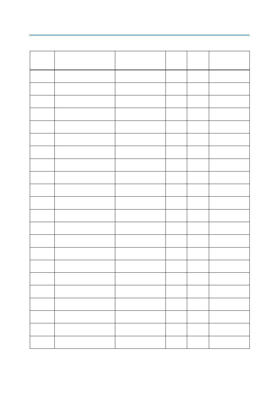
Table 2–5. MAX II Device Pin-out (Part 3 of 9)
MAX II
Pin Number
Description
Schematic Signal Name
I/O
Standard
Stratix III
Pin
Number
Other Connections