Altera Stratix III Development Board User Manual
Page 51
Chapter 2: Board Components
2–43
Components and Interfaces
May 2013
Altera Corporation
Stratix III 3SL150 Development Board
Reference Manual
Section 2.2.5 of the HSMC Specification recommends that dedicated clock inputs are
used for the differential LVDS clocks (LVDS CLK/CMOS) on pin pairs (96, 98) and
(156, 158) of the HSMC connector. The specification makes CLKIN2p/n the priority as
such the Stratix III board has a standard LVDS input pair due to lack of input clock
resources. This means that the clock driven into CLKIN1p/n from the HSMC cannot be
routed to a PLL. This limitation is true for both HSMC Port A and HSMC Port B.
If you must use another clock, you can drive the clock to the SMA output of the board,
then attach a cable from the SMA output to the SMA input. In this case, assign the
Stratix III pin that corresponds to the SMA input as your clock.
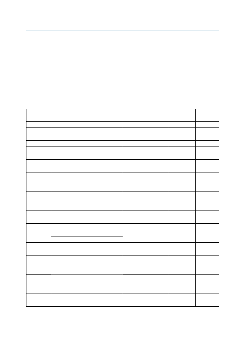
lists the HSMC Port A interface signal name, description, and signal type.
Table 2–41. HSMC Port A Interface Signal Name, Description, and Type (Part 1 of 3)
Board
Reference
Description
Schematic
Signal Name
I/O
Standard
Stratix III
Pin Number
J18 pin 33
Management serial data
HSMA_SDA
2.5 V
P8
J18 pin 34
Management serial clock
HSMA_SCL
2.5 V
AA32
J18 pin 35
JTAG clock signal
FPGA_JTAG_TCK
2.5 V
F30
J18 pin 36
JTAG mode select signal
FPGA_JTAG_TMS
2.5 V
N/A
J18 pin 37
JTAG data output
HSMA_JTAG_TDO
2.5 V
N/A
J18 pin 38
JTAG data input
HSMA_JTAG_TDI
2.5 V
N/A
J18 pin 39
Dedicated CMOS clock out
HSMA_CLK_OUT0
2.5 V
AD28
J18 pin 40
Dedicated CMOS clock in
HSMA_CLK_IN0
2.5 V
W10
J18 pin 41
Dedicated CMOS I/O bit 0
HSMA_D0
2.5 V
AK9
J18 pin 42
Dedicated CMOS I/O bit 1
HSMA_D1
2.5 V
AJ9
J18 pin 43
Dedicated CMOS I/O bit 2
HSMA_D2
2.5 V
AL7
J18 pin 44
Dedicated CMOS I/O bit 3
HSMA_D3
2.5 V
AL9
J18 pin 47
LVDS TX or CMOS I/O bit 0
HSMA_TX_P0
LVDS or 2.5 V
AC11
J18 pin 48
LVDS RX or CMOS I/O bit 0
HSMA_RX_P0
LVDS or 2.5 V
AJ4
J18 pin 49
LVDS TX or CMOS I/O bit 0
HSMA_TX_N0
LVDS or 2.5 V
AB10
J18 pin 50
LVDS RX or CMOS I/O bit 0
HSMA_RX_N0
LVDS or 2.5 V
AJ3
J18 pin 53
LVDS TX or CMOS I/O bit 1
HSMA_TX_P1
LVDS or 2.5 V
AC9
J18 pin 54
LVDS RX or CMOS I/O bit 1
HSMA_RX_P1
LVDS or 2.5 V
AG4
J18 pin 55
LVDS TX or CMOS I/O bit 1
HSMA_TX_N1
LVDS or 2.5 V
AC8
J18 pin 56
LVDS RX or CMOS I/O bit 1
HSMA_RX_N1
LVDS or 2.5 V
AG3
J18 pin 59
LVDS TX or CMOS I/O bit 2
HSMA_TX_P2
LVDS or 2.5 V
AH5
J18 pin 60
LVDS RX or CMOS I/O bit 2
HSMA_RX_P2
LVDS or 2.5 V
AM2
J18 pin 61
LVDS TX or CMOS I/O bit 2
HSMA_TX_N2
LVDS or 2.5 V
AH4
J18 pin 62
LVDS RX or CMOS I/O bit 2
HSMA_RX_N2
LVDS or 2.5 V
AM1
J18 pin 65
LVDS TX or CMOS I/O bit 3
HSMA_TX_P3
LVDS or 2.5 V
AE8
J18 pin 66
LVDS RX or CMOS I/O bit 3
HSMA_RX_P3
LVDS or 2.5 V
AL2
J18 pin 67
LVDS TX or CMOS I/O bit 3
HSMA_TX_N3
LVDS or 2.5 V
AE7
J18 pin 68
LVDS RX or CMOS I/O bit 3
HSMA_RX_N3
LVDS or 2.5 V
AL1
J18 pin 71
LVDS TX or CMOS I/O bit 4
HSMA_TX_P4
LVDS or 2.5 V
AF6