Altera Stratix III Development Board User Manual
Page 70
2–62
Chapter 2: Board Components
On-Board Memory
Stratix III 3SL150 Development Board
May 2013
Altera Corporation
Reference Manual
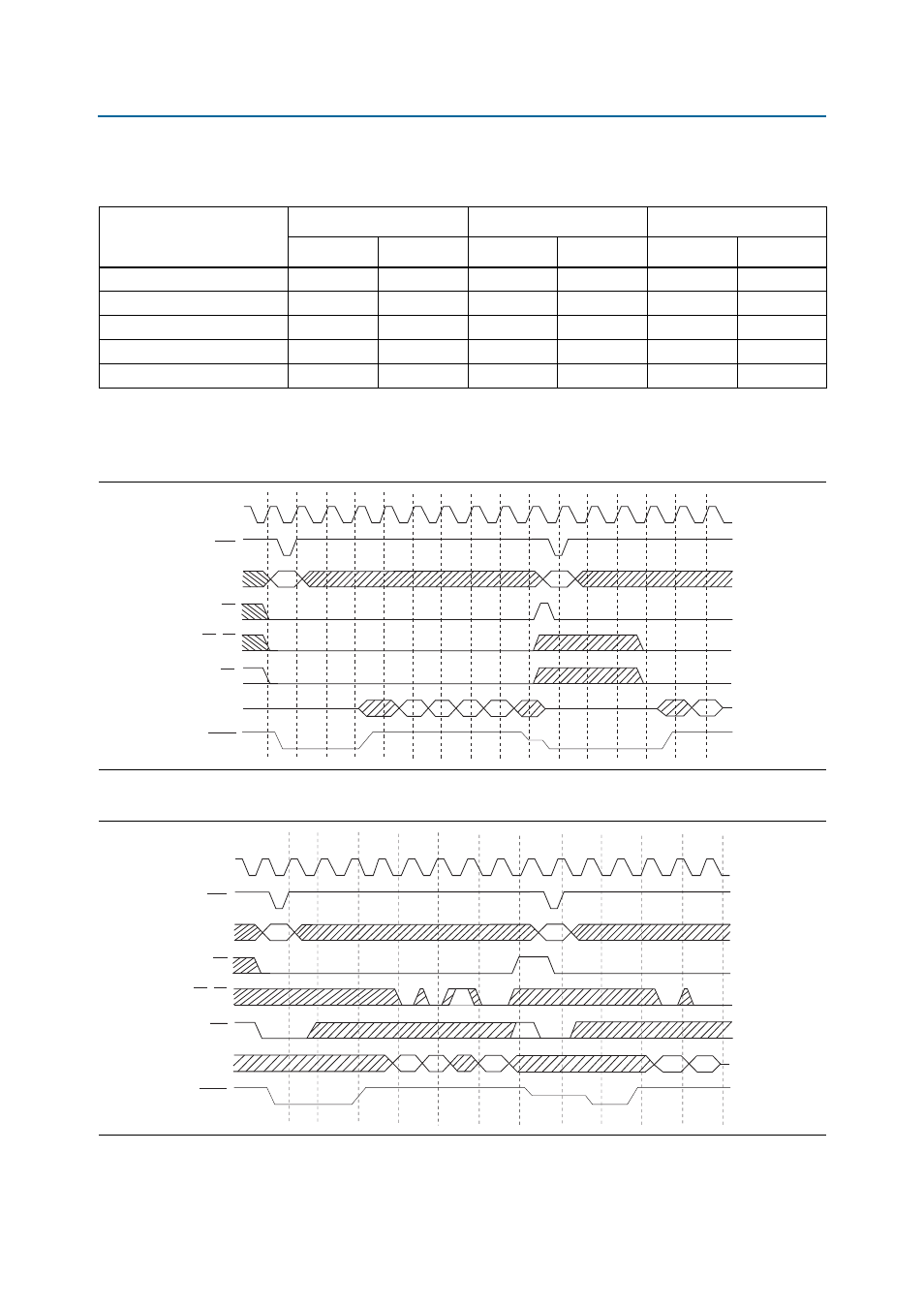
lists the Samsung device latency values based on operation frequency.
show the Samsung device read and write access
waveforms.
Table 2–53. SRAM Latency Vs. Frequency
Item
Up to 66 MHz
Up to 80 MHz
Up to 104 MHz
Fixed
Variable
Fixed
Variable
Fixed Variable
Latency set (A11:A10:A9)
4(0:0:1)
2(1:0:0)
5(0:1:0)
3(0:0:0)
7(1:0:1)
4(0:0:1)
Read latency (min)
4
2/4
5
3/5th
7
4/7
First read data fetch clock
5th
3rd/5th
6th
4th/6th
8th
5th/8th
Write latency (min)
2
2
3
3
4
4
First write data loading clock
3rd
3rd
3rd
4th
5th
5th
Figure 2–18. SRAM Read Timing Waveforms
0
1
2
3
4
5
6
7
8
9
10
11
12
13
14
Data Out
OE
ADDR
ADV
CLK
WAIT
CS
UB, LB
Figure 2–19. SRAM Write Timing Waveforms
0
1
2
3
4
5
6
7
8
9
10
11
12
13
14
Data In
WE
UB, LB
CS
ADDR
ADV
CLK
WAIT
- MAX 10 JTAG (15 pages)
- MAX 10 Power (21 pages)
- Unique Chip ID (12 pages)
- Remote Update IP Core (43 pages)
- Device-Specific Power Delivery Network (28 pages)
- Device-Specific Power Delivery Network (32 pages)
- Hybrid Memory Cube Controller (69 pages)
- ALTDQ_DQS IP (117 pages)
- MAX 10 Embedded Memory (71 pages)
- MAX 10 Embedded Multipliers (37 pages)
- MAX 10 Clocking and PLL (86 pages)
- MAX 10 FPGA (26 pages)
- MAX 10 FPGA (56 pages)
- USB-Blaster II (22 pages)
- GPIO (22 pages)
- LVDS SERDES (27 pages)
- User Flash Memory (33 pages)
- ALTDQ_DQS2 (100 pages)
- Avalon Tri-State Conduit Components (18 pages)
- Cyclone V Avalon-MM (166 pages)
- Cyclone III FPGA Starter Kit (36 pages)
- Cyclone V Avalon-ST (248 pages)
- Stratix V Avalon-ST (286 pages)
- Stratix V Avalon-ST (293 pages)
- DDR3 SDRAM High-Performance Controller and ALTMEMPHY IP (10 pages)
- Arria 10 Avalon-ST (275 pages)
- Avalon Verification IP Suite (224 pages)
- Avalon Verification IP Suite (178 pages)
- FFT MegaCore Function (50 pages)
- DDR2 SDRAM High-Performance Controllers and ALTMEMPHY IP (140 pages)
- Floating-Point (157 pages)
- Integer Arithmetic IP (157 pages)
- Embedded Peripherals IP (336 pages)
- JESD204B IP (158 pages)
- Low Latency Ethernet 10G MAC (109 pages)
- LVDS SERDES Transmitter / Receiver (72 pages)
- Nios II Embedded Evaluation Kit Cyclone III Edition (3 pages)
- Nios II Embedded Evaluation Kit Cyclone III Edition (80 pages)
- IP Compiler for PCI Express (372 pages)
- Parallel Flash Loader IP (57 pages)
- Nios II C2H Compiler (138 pages)
- RAM-Based Shift Register (26 pages)
- RAM Initializer (36 pages)
- Phase-Locked Loop Reconfiguration IP Core (51 pages)
- DCFIFO (28 pages)