Altera Stratix III Development Board User Manual
Page 50
2–42
Chapter 2: Board Components
Components and Interfaces
Stratix III 3SL150 Development Board
May 2013
Altera Corporation
Reference Manual
f
For more information about the HSMC specification such as signaling standards,
signal integrity, compatible connectors, and mechanical information, visit
www.altera.com
.
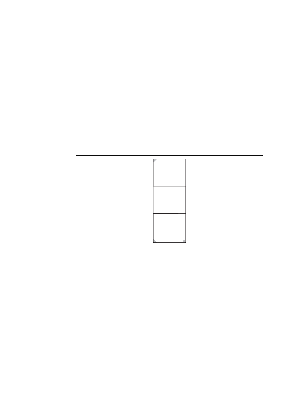
The HSMC connector has 172 total pins, including 120 signal pins, 39 power pins, and
13 ground pins. The ground pins are located between the two rows of signal and
power pins, acting as both shield and reference. The HSMC host connector is based on
the 0.5 mm-pitch QSH/QTH family of high-speed, board-to-board connectors from
Samtec. There are three banks in this connector. Bank 1 has every third pin removed as
it is done in the QSH-DP/QTH-DP series. Banks 2 and 3 have all of the pins
populated as it is done in the QSH/QTH series.
The Stratix III development board does not use bank 1 transceiver signals intended
for clock-data-recover (CDR) applications such as PCI Express and Rapid I/O
©.
These
32 pins are left floating. Banks 2 and 3 are fully supported and can be used in two
different configurations, as shown in
.
The HSMC interface has programmable bi-directional I/O pins that can be used as
2.5-V LVCMOS, which is 3.3-V LVTTL-compatible. These pins can also be used as
various differential I/O standards including, but not limited to LVDS, mini-LVDS,
and RSDS with up to 17-channels full-duplex.
1
As noted in the HSMC specification, LVDS and single-ended I/O standards are only
guaranteed to function when mixed according to either the generic single-ended
pin-out or the generic differential pin-out.
For the Stratix III FPGA Development Kit, there is only one clock per HSMC interface
that can drive a PLL. If you want to drive a PLL from the HSMC interface make sure
you use either HSMA_CLK_P2 for Port A or HSMB_CLK_P2 for Port B.
Section 2.2.4 of the HSMC Specification recommends that a dedicated clock input be
used for the single-ended clock (CMOS CLK) on pin 40 of the HSMC connector. The
Stratix III board uses a regular input pin due to lack of input clock resources. This
means that clocks driven from the HSMC cannot be routed to a PLL. This limitation is
true for both HSMC Port A and HSMC Port B.
Figure 2–16. HSMC Signal and Bank Diagram
Bank 3
Power
D(79.40)
-or-
LVDS
CLKIN2, CLKOUT2
Bank 2
Power
D(39:0)
-or-
D[3:0] + LVDS
CLKIN1, CLKOUT1
Bank 1
8 TX Channels CDR
8 RX Channels CDR
JTAG
SMBus
CLKIN0, CLKOUT0