Development board block diagram, Handling the board – Altera Arria V GX Starter Board User Manual
Page 8
1–4
Chapter 1: Overview
Development Board Block Diagram
Arria V GX Starter Board
November 2013
Altera Corporation
Reference Manual
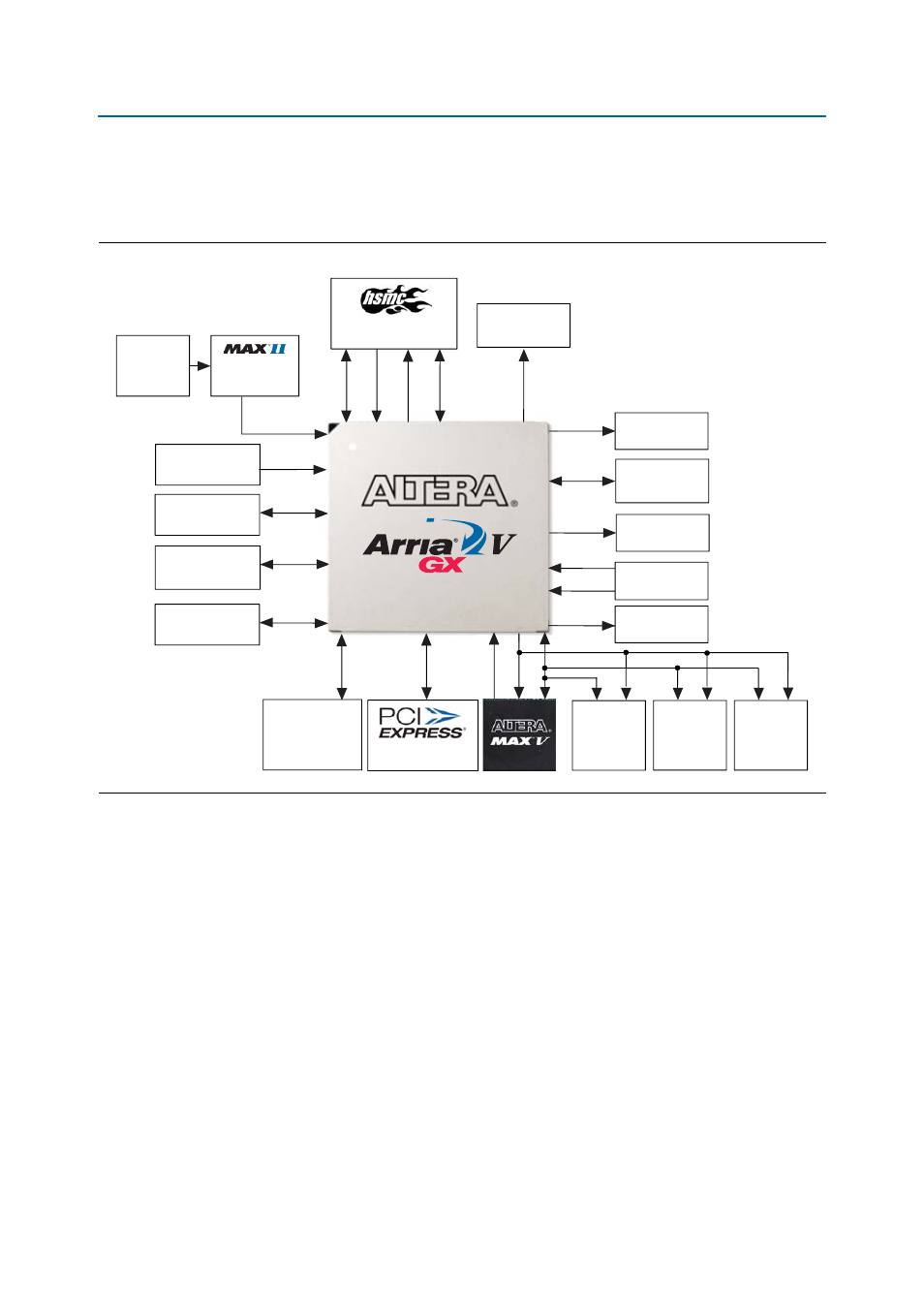
Development Board Block Diagram
shows a block diagram of the Arria V GX starter board.
Handling the Board
When handling the board, it is important to observe the following static discharge
precaution:
c
Without proper anti-static handling, the board can be damaged. Therefore, use
anti-static handling precautions when touching the board.
Figure 1–1. Arria V GX Starter Board Block Diagram
Port A
LVDS/Single-Ended
256-MB
DDR3
2x16 LCD
HDMI
TX
Push buttons
LEDs
2-MB
SSRAM
128-MB
Flash
128-MB
Flash
x8 Edge
Trigger SMA
Out
REFCLK SMA
In
Gigabit Ethernet
PHY
Embedded
USB-Blaster II
Type-B
USB 2.0
XCVR x1
SDI
TX/RX
XCVR x1
x1
x4 XVCR
x11
XCVR
SMA Out & In
x1 XCVR
x32
x32
x16
x16
x4
x4
x3
ADDR x27
DATA x32
CONFIG x16
XVCR x8
x80
CLKIN x3
CLKOUT x3
XCVR x8
JTAG Chain
x1 LVPECL
Programmable
Oscillator
50 M, 125 M
x10
x
7
6
C
L
5AGXFB3H4F35C4N
5M2210ZF256C4N
- MAX 10 JTAG (15 pages)
- MAX 10 Power (21 pages)
- Unique Chip ID (12 pages)
- Remote Update IP Core (43 pages)
- Device-Specific Power Delivery Network (28 pages)
- Device-Specific Power Delivery Network (32 pages)
- Hybrid Memory Cube Controller (69 pages)
- ALTDQ_DQS IP (117 pages)
- MAX 10 Embedded Memory (71 pages)
- MAX 10 Embedded Multipliers (37 pages)
- MAX 10 Clocking and PLL (86 pages)
- MAX 10 FPGA (26 pages)
- MAX 10 FPGA (56 pages)
- USB-Blaster II (22 pages)
- GPIO (22 pages)
- LVDS SERDES (27 pages)
- User Flash Memory (33 pages)
- ALTDQ_DQS2 (100 pages)
- Avalon Tri-State Conduit Components (18 pages)
- Cyclone V Avalon-MM (166 pages)
- Cyclone III FPGA Starter Kit (36 pages)
- Cyclone V Avalon-ST (248 pages)
- Stratix V Avalon-ST (286 pages)
- Stratix V Avalon-ST (293 pages)
- DDR3 SDRAM High-Performance Controller and ALTMEMPHY IP (10 pages)
- Arria 10 Avalon-ST (275 pages)
- Avalon Verification IP Suite (224 pages)
- Avalon Verification IP Suite (178 pages)
- FFT MegaCore Function (50 pages)
- DDR2 SDRAM High-Performance Controllers and ALTMEMPHY IP (140 pages)
- Floating-Point (157 pages)
- Integer Arithmetic IP (157 pages)
- Embedded Peripherals IP (336 pages)
- JESD204B IP (158 pages)
- Low Latency Ethernet 10G MAC (109 pages)
- LVDS SERDES Transmitter / Receiver (72 pages)
- Nios II Embedded Evaluation Kit Cyclone III Edition (3 pages)
- Nios II Embedded Evaluation Kit Cyclone III Edition (80 pages)
- IP Compiler for PCI Express (372 pages)
- Parallel Flash Loader IP (57 pages)
- Nios II C2H Compiler (138 pages)
- RAM-Based Shift Register (26 pages)
- RAM Initializer (36 pages)
- Phase-Locked Loop Reconfiguration IP Core (51 pages)
- DCFIFO (28 pages)