Clock circuitry, On-board oscillators, Clock circuitry –20 – Altera Arria V GX Starter Board User Manual
Page 28: On-board oscillators –20
2–20
Chapter 2: Board Components
Clock Circuitry
Arria V GX Starter Board
November 2013
Altera Corporation
Reference Manual
Clock Circuitry
This section describes the board's clock inputs and outputs.
On-Board Oscillators
The starter board includes programmable oscillators with a frequency of 100-MHz,
125-MHz, 156.25-MHz, and 409.60-MHz.
shows the default frequencies of all external clocks going to the Arria V GX
starter board.
Table 2–14
lists the oscillators, its I/O standard, and voltages required for the starter
board.
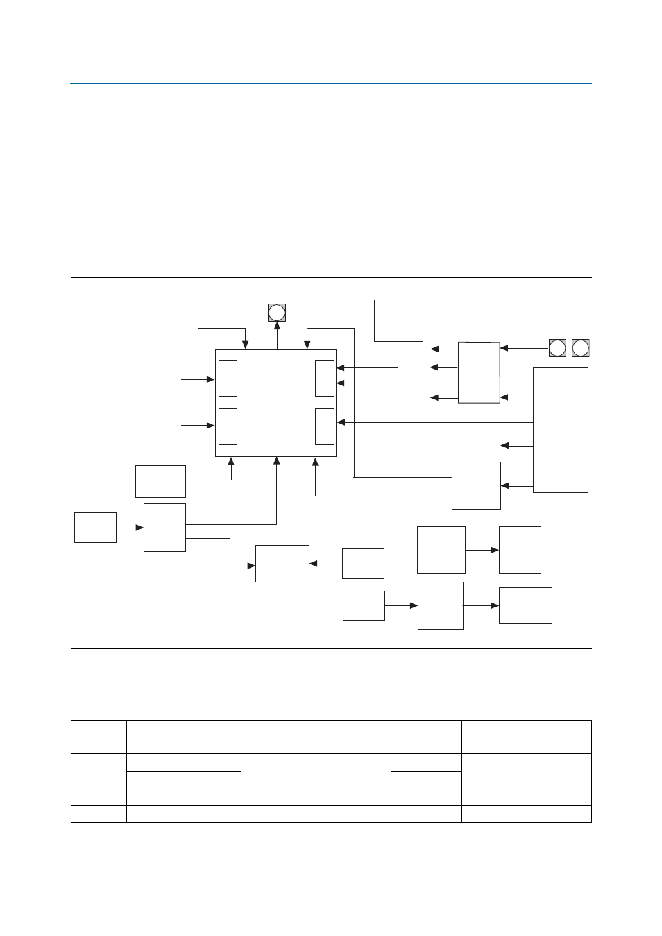
Figure 2–7. Arria V GX Starter Board Clocks
SMA
SMA
SMA
Bank Top
CH0 125 MHz
CH1 409.6 MHz
CH2 156.25 MHz
CH3 100 MHz
Si5338
x4 LVDS Output
Bank Bottom
Bank L1
Bank R1
2 Unused Channels
HSMC x8
HDMI x3
SMA x1
SDI x1
PCIe x8
Enet
DDR3 x32 UniOHY, User I/O
User I/O, HSMC VIO, Enet, HDMI
Bank R0
IDT5T9306
Clock Fan-Out
x4 LVDS
NB6L11SMNG
Clock Fan-Out
x2 LVDS
100 MHz
CH0
Si5338
CH2
Si5338
Si511
125.0 MHz LVDS
Fixed Oscillator
Si510 SE
50 MHz Fixed
Oscillator
Si510 SE
50 MHz Fixed
Oscillator
SL18860DC
Clock Fan-Out
x4 SE 50 MHz
MAX V CPLD
System Controller
Arria V FPGA
FA-128
24.0 MB-W
24 MHz XTAL
CY7C68013A
USB
Microcontroller
MAX II CPLD
Embedded
USB-Blaster
10/100/1000
Base-T
Ethernet PHY
88E1111
SG-310DF
25.0 M-B3
25 MHz
Fixed Oscillator
Bank
R1
Bank
R0
Bank
L1
Bank
L0
Si571
LVDS VCXO
148.5 MHz and
148.35 MHz
Trigger Out
SMA
LVPECL
Clock input
Table 2–14. On-Board Oscillators
Source
Schematic Signal Name
Frequency
I/O Standard
Arria V GX Pin
Number
Application
X4
CLKIN_50_TOP
50.000 MHz
2.5V CMOS
A16
Nios II and MAX V
CLKIN_50_BOT
AP29
CLKIN_50_MAXV
—
X3
CLLK_CONFIG
100.000 MHz
2.5V CMOS
—
Fast FPGA configuration