Altera Arria V GX Starter Board User Manual
Page 14

2–6
Chapter 2: Board Components
Featured Device: Arria V GX FPGA
Arria V GX Starter Board
November 2013
Altera Corporation
Reference Manual
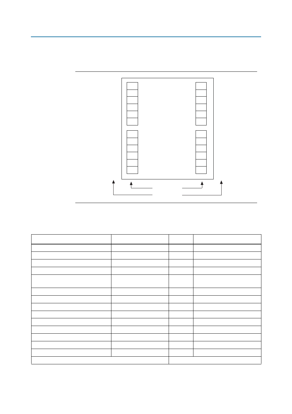
illustrates the transceiver channels on the left and right side of the
Arria V GX 5AGXFB3H4F35C4N device in the 1152-pin FBGA package.
lists the Arria V GX device I/O and transceiver pin count and usage by
function on the board.
Figure 2–3. Arria V GX Device Transceiver Bank Diagram
Transceiver Bank
Channels Per Bank
5AGXFB3H4F35
CH 0
CH 1
CH 2
CH 3
CH 4
CH 5
CH 0
CH 1
CH 2
CH 3
CH 4
CH 5
GXB_L0
GXB_L1
GXB_R1
GXB_R0
CH 0
CH 1
CH 2
CH 3
CH 4
CH 5
CH 0
CH 1
CH 2
CH 3
CH 4
CH 5
Table 2–4. Arria V GX Device I/O and Transceiver Pin Count
Function
I/O Standard
I/O Count
Special Pins
DDR3
1.5-V SSTL
70
One differential x4 DQS pin
Flash, SSRAM, and MAX V FSM bus
2.5-V CMOS
87
—
MAX V CPLD 5M2210 System Controller
2.5-V CMOS
10
—
PCI Express x8
2.5-V CMOS + XCVR
42
One reference clock
HSMA port A
2.5-V CMOS + LVDS + XCVR
116
Eight XCVR, 17 LVDS, six clock
inputs/outputs, I
2
C
Gigabit Ethernet
2.5-V CMOS + LVDS
20
One LVDS
On-Board USB-Blaster II
2.5-V CMOS
20
—
SDI video
2.5-V CMOS
15
One reference clock
HDMI video
2.5-V CMOS
14
One reference clock
Push buttons
2.5-V CMOS
4
One DEV_CLRn
DIP switches
2.5-V CMOS
4
—
Character LCD
2.5-V CMOS
11
—
LEDs
2.5-V CMOS
7
—
Clock or Oscillators
2.5-V CMOS + LVDS + PCML
21
11 reference clock
Total I/O Used:
441
