Altera Arria V GX Starter Board User Manual
Page 16
2–8
Chapter 2: Board Components
MAX V CPLD 5M2210 System Controller
Arria V GX Starter Board
November 2013
Altera Corporation
Reference Manual
C9
CLOCK_SCL
2.5-V
Programmable oscillator I
2
C clock
D9
CLOCK_SDA
2.5-V
Programmable oscillator I
2
C data
D10
CPU_RESETN
2.5-V
FPGA reset push button
M1
EXTRA_SIG0
2.5-V
USB-Blaster II interface. Reserved for future use.
T13
EXTRA_SIG1
2.5-V
USB-Blaster II interface. Reserved for future use.
T15
EXTRA_SIG2
2.5-V
USB-Blaster II interface. Reserved for future use.
A2
FACTORY_LOAD
2.5-V
DIP switch to load factory or user design at power-up
R14
FACTORY_REQUEST
2.5-V
On-Board USB-Blaster II request to send FACTORY
command
N12
FACTORY_STATUS
2.5-V
On-Board USB-Blaster II FACTORY command status
C8
FAN_FORCE_ON
2.5-V
DIP switch to on or off the fan
N7
FLASH_ADVN
2.5-V
FSM bus flash memory address valid
R5
FLASH_CEN0
2.5-V
FSM bus flash memory chip enable 0
M7
FLASH_CEN1
2.5-V
FSM bus flash memory chip enable 1
R6
FLASH_CLK
2.5-V
FSM bus flash memory clock
M6
FLASH_OEN
2.5-V
FSM bus flash memory output enable
T5
FLASH_RDYBSYN0
2.5-V
FSM bus flash memory ready 0
R7
FLASH_RDYBSYN1
2.5-V
FSM bus flash memory ready 1
P7
FLASH_RESETN
2.5-V
FSM bus flash memory reset
N6
FLASH_WEN
2.5-V
FSM bus flash memory write enable
K1
FPGA_CONF_DONE
2.5-V
FPGA configuration done LED
D3
FPGA_CONFIG_D0
2.5-V
FPGA configuration data
C2
FPGA_CONFIG_D1
2.5-V
FPGA configuration data
C3
FPGA_CONFIG_D2
2.5-V
FPGA configuration data
E3
FPGA_CONFIG_D3
2.5-V
FPGA configuration data
D2
FPGA_CONFIG_D4
2.5-V
FPGA configuration data
E4
FPGA_CONFIG_D5
2.5-V
FPGA configuration data
D1
FPGA_CONFIG_D6
2.5-V
FPGA configuration data
E5
FPGA_CONFIG_D7
2.5-V
FPGA configuration data
F3
FPGA_CONFIG_D8
2.5-V
FPGA configuration data
E1
FPGA_CONFIG_D9
2.5-V
FPGA configuration data
F4
FPGA_CONFIG_D10
2.5-V
FPGA configuration data
F2
FPGA_CONFIG_D11
2.5-V
FPGA configuration data
F1
FPGA_CONFIG_D12
2.5-V
FPGA configuration data
F6
FPGA_CONFIG_D13
2.5-V
FPGA configuration data
G2
FPGA_CONFIG_D14
2.5-V
FPGA configuration data
G3
FPGA_CONFIG_D15
2.5-V
FPGA configuration data
N3
FPGA_CVP_CONFDONE
2.5-V
FPGA configuration via protocol done LED
J3
FPGA_DCLK
2.5-V
FPGA configuration clock
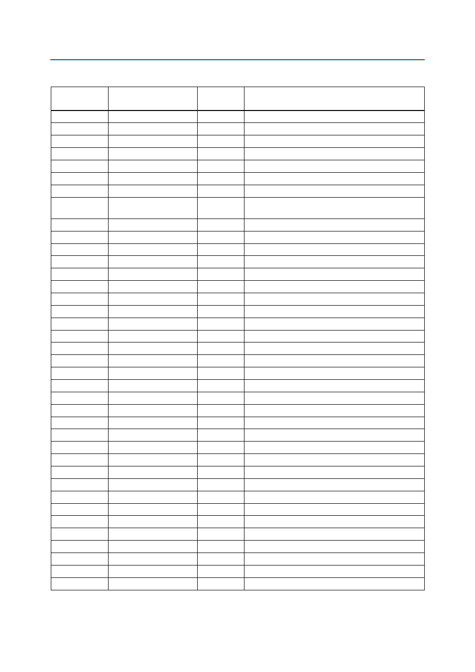
Table 2–5. MAX V CPLD 5M2210 System Controller Device Pin-Out (Part 2 of 6)
Board
Reference (U15)
Schematic Signal Name
I/O Standard
Description